-
UCC28180 Programmable Frequency, Continuous Conduction Mode (CCM), Boost Power Factor Correction (PFC) Controller
- 1 Features
- 2 Applications
- 3 Description
- 4 Revision History
- 5 Description (Continued)
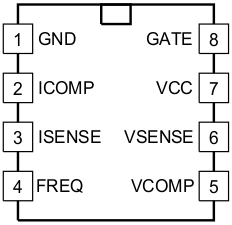
- 6 Pin Configuration and Functions
- 7 Specifications
-
8 Detailed Description
- 8.1 Overview
- 8.2 Functional Block Diagram
- 8.3
Feature Description
- 8.3.1 Soft Start
- 8.3.2 System Protection
- 8.3.3 VCC Undervoltage LockOut (UVLO)
- 8.3.4 Output Overvoltage Protection (OVP)
- 8.3.5 Open Loop Protection/Standby (OLP/Standby)
- 8.3.6 ISENSE Open-Pin Protection (ISOP)
- 8.3.7 ICOMP Open-Pin Protection (ICOMPP)
- 8.3.8 FAULT Protection
- 8.3.9 Output Overvoltage Detection (OVD), Undervoltage Detection (UVD) and Enhanced Dynamic Response (EDR)
- 8.3.10 Overcurrent Protection
- 8.3.11 Soft Overcurrent (SOC)
- 8.3.12 Peak Current Limit (PCL)
- 8.3.13 Current Sense Resistor, RISENSE
- 8.3.14 ISENSE Pin
- 8.3.15 Gate Driver
- 8.3.16 Current Loop
- 8.3.17 ISENSE and ICOMP Functions
- 8.3.18 Pulse Width Modulator
- 8.3.19 Control Logic
- 8.3.20 Voltage Loop
- 8.3.21 Output Sensing
- 8.3.22 Voltage Error Amplifier
- 8.3.23 Non-Linear Gain Generation
- 8.4 Device Functional Modes
-
9 Application and Implementation
- 9.1 Application Information
- 9.2
Typical Application
- 9.2.1 Design Requirements
- 9.2.2
Detailed Design Procedure
- 9.2.2.1 Current Calculations
- 9.2.2.2 Switching Frequency
- 9.2.2.3 Bridge Rectifier
- 9.2.2.4 Inductor Ripple Current
- 9.2.2.5 Input Capacitor
- 9.2.2.6 Boost Inductor
- 9.2.2.7 Boost Diode
- 9.2.2.8 Switching Element
- 9.2.2.9 Sense Resistor
- 9.2.2.10 Output Capacitor
- 9.2.2.11 Output Voltage Set Point
- 9.2.2.12 Loop Compensation
- 9.2.3 Application Curve
- 10Power Supply Recommendations
- 11Layout
- 12Device and Documentation Support . .
- 13Mechanical, Packaging, and Orderable Information
- IMPORTANT NOTICE
Package Options
Mechanical Data (Package|Pins)
- D|8
Thermal pad, mechanical data (Package|Pins)
Orderable Information
UCC28180 Programmable Frequency, Continuous Conduction Mode (CCM), Boost Power Factor Correction (PFC) Controller
1 Features
- 8-Pin Solution (No AC Line Sensing Needed)
- Wide Range Programmable Switching Frequency (18 kHz to 250 kHz for MOSFET and IGBT-based PFC Converters)
- Trimmed Current Loop Circuits for Low iTHD
- Reduced Current Sense Threshold (Minimizes Power Dissipation in Shunt)
- Average Current-Mode Control
- Soft Over Current and Cycle-by-Cycle Peak Current Limit Protection
- Output Overvoltage Protection With Hysteresis Recovery
- Audible Noise Minimization Circuitry
- Open Loop Detection
- Enhance Dynamic Response During Output Overvoltage and Undervoltage Conditions
- Maximum Duty Cycle of 96% (Typical)
- Burst Mode for No Load Regulation
- VCC UVLO, Low ICC Start-Up (< 75 µA)
2 Applications
- Universal AC Input, CCM Boost PFC Converters in 100-W to Few-kW Range
- Server and Desktop Power Supplies
- White Good Appliances (Air Conditioners, Refrigerators)
- Industrial Power Supplies (DIN Rail)
- Flat Panel (PDP, LCD, and LED) TVs
3 Description
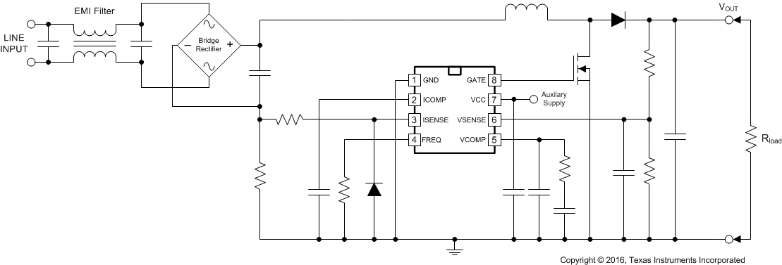
The UCC28180 is a flexible and easy-to-use, 8-pin, active Power-Factor Correction (PFC) controller that operates under Continuous Conduction Mode (CCM) to achieve high Power Factor, low current distortion and excellent voltage regulation of boost pre-regulators in AC - DC front-ends. The controller is suitable for universal AC input systems operating in 100-W to few-kW range with the switching frequency programmable between 18 kHz to 250 kHz, to conveniently support both power MOSFET and IGBT switches. An integrated 1.5-A and 2-A (SRC-SNK) peak gate drive output, clamped internally at 15.2 V (typical), enables fast turn-on, turn-off, and easy management of the external power switch without the need for buffer circuits.
Low-distortion wave shaping of the input current using average current mode control is achieved without input line sensing, reducing the external component count. In addition, the controller features reduced current sense thresholds to facilitate the use of small-value shunt resistors for reduced power dissipation, especially important in high-power systems. To enable low current distortion, the controller also features trimmed internal current loop regulation circuits for eliminating associated inaccuracies.
Device Information(1)
| PART NUMBER | PACKAGE | BODY SIZE (NOM) |
|---|---|---|
| UCC28180 | SOIC (8) | 4.90 mm × 3.91 mm |
- For all available packages, see the orderable addendum at the end of the datasheet.
space
space
space
4 Revision History
Changes from C Revision (April 2016) to D Revision
- Changed the correct page number in the C Revision History of the diode addition to the Functional Block Diagram.Go
- Changed text value of 0.538 to 0.366 to align with Equation 85. Updated change was implemented in the C revision and recorded in the D revision.Go
- Added D4 to Table 2. Updated change was implemented in the C revision and recorded in the D revision.Go
- Added Receiving Notification of Documentation Updates.Go
- Added Community Resources.Go
Changes from B Revision (December 2014) to C Revision
- Added a diode to the Typical Application Schematic image.Go
- Changed ICC Standby current MAX rate from 2.95 mA to 3.47 mA.Go
- Changed ISENSE threshold, soft over current (SOC) TYP value from –0.295 V to –0.285 V.Go
- Changed Maximum current under EDR operation MAX rating from –241 µA to –275 µA. Go
- Added a diode to the Functional Block Diagram.Go
- Added Diode to Soft Overcurrent/Peak-Current Limit image.Go
- Added ISENSE Pin section. Go
- Added diode to the Design Example Schematic image. Go
- Changed Equation 101 3kHz to 5kHz.Go
- Changed Recommended Layout for UCC28180 image.Go
Changes from A Revision (November 2013) to B Revision
- Added ESD Rating table, Feature Description section, Device Functional Modes, Application and Implementation section, Power Supply Recommendations section, Layout section, Device and Documentation Support section, and Mechanical, Packaging, and Orderable Information section Go
5 Description (Continued)
Simple external networks allow for flexible compensation of the current and voltage control loops. In addition, UCC28180 offers an enhanced dynamic response circuit that is based on the voltage feedback signal to deliver improved response under fast load transients, both for output overvoltage and undervoltage conditions. An unique VCOMP discharge circuit provided in UCC28180 is activated whenever the voltage feedback signal exceeds VOVP_L thus allowing a chance for the control loop to stabilize quickly and avoid encountering the overvoltage protection function when PWM shutoff can often cause audible noise. Controlled soft start gradually regulates the input current during start-up and reduces stress on the power switches. Numerous system-level protection features available in the controller include VCC UVLO, peak current limit, soft overcurrent, output open-loop detection, output overvoltage protection and open-pin detection (VISNS). A trimmed internal reference provides accurate protection thresholds and regulation set-point. The user can control low-power standby mode by pulling the VSENSE pin below 0.82 V.
6 Pin Configuration and Functions

Pin Functions
| PIN | I/O | DESCRIPTION | |
|---|---|---|---|
| NAME | NO. | ||
| GATE | 8 | O | Gate Drive: Integrated push-pull gate driver for one or more external power MOSFETs. Typical 2.0-A sink and 1.5-A source capability. Output voltage is typically clamped at 15.2 V (typical). |
| GND | 1 | Ground: device ground reference. | |
| ICOMP | 2 | O | Current Loop Compensation: Transconductance current amplifier output. A capacitor connected to GND provides compensation and averaging of the current sense signal in the current control loop. The controller is disabled if the voltage on ICOMP is less than 0.2 V, (ICOMPP protection function). |
| ISENSE | 3 | I | Inductor Current Sense: Input for the voltage across the external current sense resistor, which represents the instantaneous current through the PFC boost inductor. This voltage is averaged by the current amplifier to eliminate the effects of ripple and noise. Soft Over Current (SOC) limits the average inductor current. Cycle-by-cycle peak current limit (PCL) immediately shuts off the GATE drive if the peak-limit voltage is exceeded. An internal 2.3-µA current source pulls ISENSE above 0.085 V to shut down PFC operation if this pin becomes open-circuited, (ISOP protection function). Use a 220-Ω resistor between this pin and the current sense resistor to limit inrush-surge currents into this pin. |
| VCC | 7 | Device Supply: External bias supply input. Under-Voltage Lockout (UVLO) disables the controller until VCC exceeds a turn-on threshold of 11.5 V. Operation continues until VCC falls below the turn-off (UVLO) threshold of 9.5 V. A ceramic by-pass capacitor of 0.1 µF minimum value should be connected from VCC to GND as close to the device as possible for high-frequency filtering of the VCC voltage. | |
| VCOMP | 5 | O | Voltage Loop Compensation: Transconductance voltage error amplifier output. A resistor-capacitor network connected from this pin to GND provides compensation. VCOMP is held at GND until VCC, and VSENSE exceed their threshold voltages. Once these conditions are satisfied, VCOMP is charged until the VSENSE voltage reaches its nominal regulation level. When Enhanced Dynamic Response (EDR) is engaged, a higher transconductance is applied to VCOMP to reduce the charge or discharge time for faster transient response. Soft Start is programmed by the capacitance on this pin. VCOMP is pulled low when VCC UVLO, OLP/Standby, ICOMPP and ISOP functions are activated. |
| FREQ | 4 | O | Switching Frequency Setting: This pin allows the setting of the operating switching frequency by connecting a resistor to ground. The programmable frequency range is from 18 kHz to 250 kHz. |
| VSENSE | 6 | I | Output Voltage Sense: An external resistor-divider network connected from this pin to the PFC output voltage provides feedback sensing for regulation to the internal 5-V reference voltage. A small capacitor from this pin to GND filters high-frequency noise. Standby disables the controller and discharges VCOMP when the voltage at VSENSE drops below the Open-Loop Protection (OLP) threshold of 16.5%VREF (0.82 V). An internal 100-nA current source pulls VSENSE to GND during pin disconnection. Enhanced Dynamic Response (EDR) rapidly returns the output voltage to its normal regulation level when a system line or load step causes VSENSE to rise above 105% or fall below 95% of the reference voltage. Two level Output Over-Voltage Protection (OVP): a 4-kΩ resistor connects VCOMP to ground to rapidly discharge VCOMP when VSENSE exceeds 107% (VOVP_L) of the reference voltage. If VSENSE exceeds 109% (VOVP_H) of the reference voltage, GATE output will be disabled until VSENSE drops below 102% of the reference voltage. |
