-
UCC28C5x-Q1 Automotive Low-Power Current-Mode High-Performance PWM Controller for Si and SiC MOSFETs SLUSEV2C June 2022 – March 2023 UCC28C50-Q1 , UCC28C51-Q1 , UCC28C52-Q1 , UCC28C53-Q1 , UCC28C54-Q1 , UCC28C55-Q1 , UCC28C56H-Q1 , UCC28C56L-Q1 , UCC28C57H-Q1 , UCC28C57L-Q1 , UCC28C58-Q1 , UCC28C59-Q1
PRODUCTION DATA
-
UCC28C5x-Q1 Automotive Low-Power Current-Mode High-Performance PWM Controller for Si and SiC MOSFETs
- 1 Features
- 2 Applications
- 3 Description
- 4 Revision History
- 5 Device Comparison Table
- 6 Pin Configuration and Functions
- 7 Specifications
-
8 Detailed Description
- 8.1 Overview
- 8.2 Functional Block Diagram
- 8.3 Feature Description
- 8.4 Device Functional Modes
-
9 Application and Implementation
- 9.1 Application Information
- 9.2
Typical Application
- 9.2.1 Design Requirements
- 9.2.2
Detailed Design Procedure
- 9.2.2.1 Primary-to-Secondary Turns Ratio of the Flyback Transformer (NPS)
- 9.2.2.2 Primary Magnetizing Inductance of the Flyback Transformer (LM)
- 9.2.2.3 Number of Turns of the Flyback Transformer Windings
- 9.2.2.4 Current Sense Resistors (R24, R25) and Current Limiting
- 9.2.2.5 Primary Clamp Circuit (D7, D1, D3, R2, R28) to Limit Voltage Stress
- 9.2.2.6 Primary-Side Current Stress and Input Capacitor Selection
- 9.2.2.7 Secondary-Side Current Stress and Output Capacitor Selection
- 9.2.2.8 VDD Capacitors (C12, C18)
- 9.2.2.9 Gate Drive Network (R14, R16, Q6)
- 9.2.2.10 VREF Capacitor (C18)
- 9.2.2.11 RT/CT Components (R12, C15)
- 9.2.2.12 HV Start-Up Circuitry for VDD (Q1, Q2, D2, D4, D6, D8, R5)
- 9.2.2.13 Desensitization to CS-pin Noise by RC Filtering, Leading-Edge Blanking, and Slope Compensation
- 9.2.2.14 Voltage Feedback Compensation
- 9.2.3 Application Curves
- 9.3 PCB Layout Recommendations
- 9.4 Power Supply Recommendations
- 10Device and Documentation Support
- 11Mechanical, Packaging, and Orderable Information
- IMPORTANT NOTICE
Package Options
Mechanical Data (Package|Pins)
- D|8
Thermal pad, mechanical data (Package|Pins)
Orderable Information
UCC28C5x-Q1 Automotive Low-Power Current-Mode High-Performance PWM Controller for Si and SiC MOSFETs
1 Features
- Undervoltage lockout options to support both Si and SiC MOSFET applications
-
30-V VDD absolute maximum voltage
- 1-MHz maximum Fixed frequency oeration
- 50-μA startup current, 75-μA maximum
- Low operating current : 1.3 mA at fOSC = 52 kHz
- High operating TJ : 150℃ maximum
- Fast 35-ns cycle-by-cycle over-current limiting
- ±1-A peak driving current
- Rail-to-rail output:
- 25-ns rise time
- 20-ns fall time
- ±1% accurate 2.5-V error amplifier reference
-
Pin-to-pin compatible and drop-in replacement for UCC28C4x-Q1
- Functional Safety-Capable
- Documentation available to aid functional safety system design
- AEC-Q100 qualified with the following results
- Device temperature grade 1: -40°C to 125°C
- Device HBM classification level 2: ±2 kV
- Device CDM classification level C4B: 750 V
2 Applications
- Traction inverter HV to LV backup supply
- OBC and DC/DC converter isolated bias power supply
- HVAC compressor HV isolated power supply
- Single-ended DC converters in AC and DC EV charging equipment
3 Description
The UCC28C5x-Q1 family of devices are high performance current-mode PWM controllers which can be used to drive both Si and SiC MOSFETs in various applications. The UCC28C5x-Q1 family is a more efficient and robust version of the UCC28C4x-Q1.
The UCC28C5x-Q1 family has new UVLO thresholds that allow for reliable SiC MOSFET operation (UCC28C56-59-Q1), in addition to existing UVLO thresholds for continued Si MOSFET support (UCC28C50-55-Q1).
VDD absolute maximum voltage rating is extended from 20 V to 30 V for optimally driving the gate of 20-Vgs, 18-Vgs, or 15-Vgs SiC MOSFETs, while also allowing for the exclusion of an external LDO.
| PARAMETER | UCC28C4x-Q1 | UCC28C5x-Q1 |
|---|---|---|
| Supply current at 52 kHz | 2.3 mA | 1.3 mA |
| Startup current (max) | 100 µA | 75 µA |
| VDD abs max | 20 V | 30 V |
| Reference Voltage Accuracy | ±2% | ±1% |
| UVLO and DMAX for Si FET | 6 options | 6 options |
| UVLO and DMAX for SiC FET | none | 6 options |
- For all available packages, see the orderable addendum at the end of the data sheet.
4 Revision History
Changes from Revision B (February 2023) to Revision C (March 2023)
- Initial release of the UCC28C58-Q1 deviceGo
- Updated Available Options TableGo
- Added Link to Technical Support Go
Changes from Revision A (October 2022) to Revision B (February 2023)
- Initial release of the UCC28C55-Q1, UCC28C56L-Q1, UCC28C57L-Q1 and UCC28C57H-Q1 deviceGo
5 Device Comparison Table
| UVLO | MAXIMUM DUTY CYCLE | TEMPERATURE (TA) | ||
|---|---|---|---|---|
| TURN ON AT 14.5 V TURN OFF AT 9 V SUITABLE FOR OFF-LINE APPLICATIONS | TURN ON AT 8.4 V TURN OFF AT 7.6 V SUITABLE FOR DC/DC APPLICATIONS | TURN ON AT 7 V TURN OFF AT 6.6 V SUITABLE FOR BATTERY APPLICATIONS | ||
| UCC28C52QDRQ1 | UCC28C53QDRQ1 | UCC28C50QDRQ1 | 100% | –40°C to 125°C |
| UCC28C54QDRQ1 | UCC28C55QDRQ1 | UCC28C51QDRQ1 | 50% | |
| UVLO | MAXIMUM DUTY CYCLE | TEMPERATURE (TA) | ||
|---|---|---|---|---|
| TURN ON AT 18.8 V TURN OFF AT 15.5V Suitable for HV applications using GEN-I SiC MOSFET | TURN ON AT 18.8 V TURN OFF AT 14.5V | TURN ON AT 16 V TURN OFF AT 12.5V | ||
| UCC28C56HQDRQ1 | UCC28C56LQDRQ1 | UCC28C58QDRQ1 | 100% | –40°C to 125°C |
| UCC28C57HQDRQ1 | UCC28C57LQDRQ1 | UCC28C59QDRQ1 | 50% | |
| PART NUMBER | PACKAGE | BODY SIZE (NOM) |
|---|---|---|
| UCC28C50-Q1, UCC28C51-Q1, UCC28C52-Q1 | SOIC (8) | 4.90 mm × 3.91 mm |
| UCC28C53-Q1, UCC28C54-Q1, UCC28C55-Q1 | ||
| UCC28C56H-Q1, UCC28C56L-Q1 | ||
| UCC28C57H-Q1, UCC28C57L-Q1 | ||
| UCC28C58-Q1, UCC28C59-Q1 |
6 Pin Configuration and Functions
| PIN | I/O | DESCRIPTION | |
|---|---|---|---|
| NAME | NO. | ||
| COMP | 1 | O | This pin provides the output of the error amplifier for compensation. In addition, the COMP pin is frequently used as a control port, by utilizing a secondary-side error amplifier to send an error signal across the secondary-primary isolation boundary through an opto-isolator. The error amplifier is internally current limited so the user can command zero duty cycle by externally forcing COMP to GND. |
| CS | 3 | I | Primary-side current sense pin. The current sense pin is the noninverting input to the PWM comparator. Connect to current sensing resistor. This signal is compared to a signal proportional to the error amplifier output voltage. The PWM uses this to terminate the OUT switch conduction. A voltage ramp can be applied to this pin to run the device with a voltage mode control configuration. |
| FB | 2 | I | This pin is the inverting input to the error amplifier. FB is used to control the power converter voltage-feedback loop for stability. The noninverting input to the error amplifier is internally trimmed to 2.5 V ±1%. |
| GND | 5 | — | Ground return pin for the output driver stage and the logic level controller section. |
| OUT | 6 | O | The output of the on-chip drive stage. OUT is intended to directly drive a MOSFET. The OUT pin in the UCC28C50-Q1, UCC28C52-Q1, UCC28C53-Q1, UCC28C56H/L-Q1, and UCC28C58-Q1 is the same frequency as the oscillator, and can operate near 100% duty cycle. In the UCC28C51-Q1, UCC28C54-Q1, UCC28C55-Q1, UCC28C57H/L-Q1, and UCC28C59-Q1, the frequency of OUT is one-half that of the oscillator due to an internal T flipflop. This limits the maximum duty cycle to < 50%. Peak currents of up to 1 A are sourced and sunk by this pin. OUT is actively held low when VDD is below the turn-on threshold. |
| RT/CT | 4 | I/O |
Fixed frequency oscillator set point. Connect timing resistor (RRT) to VREF and timing capacitor (CCT) to GND from this pin to set the switching frequency. For best performance, keep the timing capacitor lead to the device GND as short and direct as possible. If possible, use separate ground traces for the timing capacitor and all other functions. The switching frequency (fSW) of the UCC28C50-Q1, UCC28C52-Q1, UCC28C53-Q1, UCC28C56H/L and UCC28C58 gate drive is equal to fOSC; the switching frequency of the UCC28C51-Q1, UCC28C54-Q1, UCC28C55-Q1, UCC28C57H/L-Q1, and UCC28C59-Q1 is equal to half of the fOSC. |
| VDD | 7 | I | Analog controller bias input that provides power to the device. Total VDD current is the sum of the quiescent VDD current and the average OUT current. A bypass capacitor, typically 0.1 µF, connected directly to GND with minimal trace length, is required on this pin. Additional capacitance at least 10 times greater than the gate capacitance of the main switching FET used in the design and 10 times greater than the capacitance on the VREF pin are also required on VDD. |
| VREF | 8 | O | 5-V reference voltage. VREF is used to provide charging current to the oscillator timing capacitor through the timing resistor. It is important for reference stability that VREF is bypassed to GND with a ceramic capacitor connected as close to the pin as possible. A minimum value of 0.1 µF ceramic is required. Additional VREF bypassing is required for external loads on VREF. No external voltage higher than specified VREF is allowed to superimposed to VREF pin Since VREF is an ouput. |
7 Specifications
7.1 Absolute Maximum Ratings
| MIN | MAX | UNIT | ||
|---|---|---|---|---|
| Input voltage | VDD | 30 | V | |
| Input current | IVDD | 30 | mA | |
| Output drive current (peak) | ±1 | A | ||
| Output energy (capacitive load), EOUT | 5 | µJ | ||
| Analog input voltage | COMP, CS, FB, RT/CT | –0.3 | 6.3 | V |
| Output driver voltage | OUT | –0.3 | 30 | |
| Reference voltage | VREF | 7 | ||
| Error amplifier output sink current | COMP | 10 | mA | |
| Total power dissipation at TA = 25°C | D package | 72.3 | °C/W | |
| Lead temperature (soldering, 10 s), TLEAD | 300 | °C | ||
| Operating junction temperature, TJ | –40 | 150 | °C | |
| Storage temperature, Tstg | –65 | 150 | °C | |
7.2 ESD Ratings
| VALUE | UNIT | |||
|---|---|---|---|---|
| V(ESD) | Electrostatic discharge | Human-body model (HBM), per AEC Q100-002(1) | ±2000 | V |
| Charged-device model (CDM), per AEC Q100-011 Section 7.2 | ±750 | |||
7.3 Recommended Operating Conditions
| MIN | MAX | UNIT | |||
|---|---|---|---|---|---|
| VVDD | Input voltage | 28 | V | ||
| VOUT | Output driver voltage | 28 | V | ||
| IOUT | Average output driver current(1) | 200 | mA | ||
| IOUT(VREF) | Reference output current(1) | –20 | mA | ||
| TJ | Operating junction temperature(1) | UCC28C5x-Q1 | –40 | 150 | °C |
TA | Operating ambient temperature(1) | UCC28C5x-Q1 | –40 | 125 | °C |
7.4 Thermal Information
| THERMAL METRIC(1) | UCC28C5x-Q1 | UNIT | |||
|---|---|---|---|---|---|
| D (SOIC) 8 PINS | |||||
| RθJA | Junction-to-ambient thermal resistance | 128.9 | °C/W | ||
| RθJC(top) | Junction-to-case (top) thermal resistance | 71.7 | °C/W | ||
| RθJB | Junction-to-board thermal resistance | 72.3 | °C/W | ||
| ψJT | Junction-to-top characterization parameter | 23.4 | °C/W | ||
| ψJB | Junction-to-board characterization parameter | 71.5 | °C/W | ||
7.5 Electrical Characteristics
| PARAMETER | TEST CONDITIONS | MIN | TYP | MAX | UNIT | |
|---|---|---|---|---|---|---|
| REFERENCE | ||||||
| VVREF | VREF voltage, initial accuracy | IOUT = 1 mA | 4.95 | 5 | 5.05 | V |
| Line regulation | VVDD = 12 V to 25 V | 0.2 | 20 | mV | ||
| Load regulation | 1 mA to 20 mA | 3 | 25 | mV | ||
| Temperature stability | See (2) | 0.2 | 0.4 | mV/°C | ||
| Total output variation | See (2) | 4.82 | 5.18 | V | ||
| VREF noise voltage | 10 Hz to 10 kHz, TJ = 25°C, see (2) | 50 | µV | |||
| Long term stability | 1000 hours, TJ = 150°C, see (2) | 5 | 25 | mV | ||
| IVREF | Output short circuit (source current) | 30 | 45 | 55 | mA | |
| OSCILLATOR | ||||||
| fOSC | Initial accuracy | TJ = 25°C, see (3) | 50.5 | 53 | 55 | kHz |
| TJ = Full Range, see (3) | 50.5 | 57 | kHz | |||
| Voltage stability | 12 V ≤ VVDD ≤ 25 V | 0.2% | 1% | |||
| Temperature stability | TJ(MIN) to TJ(MAX), see (2) | 1% | 2.5% | |||
| Amplitude | RT/CT pin peak-to-peak voltage | 1.9 | V | |||
| Discharge current | TJ = 25°C, VRT/CT = 2 V, see (4) | 7.7 | 8.4 | 9 | mA | |
| TJ = Full Range, VRT/CT = 2 V, see (4) | 7.2 | 8.4 | 9.5 | |||
| ERROR AMPLIFIER | ||||||
| VFB | Feedback input voltage, initial accuracy | TJ = 25°C, VCOMP = 2.5 V | 2.475 | 2.5 | 2.525 | V |
| Feedback input voltage, total variation | TJ = Full Range, VCOMP = 2.5 V | 2.45 | 2.5 | 2.55 | V | |
| IFB | Input bias current | VFB = 5 V, (sourcing current) | 0.1 | 2 | µA | |
| AVOL | Open-loop voltage gain | 2 V ≤ VOUT ≤ 4 V | 65 | 90 | dB | |
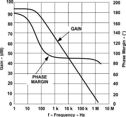
| Unity gain bandwidth | See (2) | 1 | 1.5 | MHz | ||
| PSRR | Power supply rejection ratio | 12 V ≤ VVDD ≤ 25 V | 60 | dB | ||
| Output sink current | VFB = 2.7 V, VCOMP = 1.1 V | 2 | 14 | mA | ||
| Output source current | VFB = 2.3 V, VCOMP = 5 V, (sourcing current) | 0.5 | 1 | mA | ||
| VOH | High-level COMP voltage | VFB = 2.7 V, RCOMP = 15 kΩ COMP to GND | VREF–0.2 | V | ||
| VOL | Low-level COMP voltage | VFB = 2.7 V, RCOMP = 15 kΩ COMP to VREF | 0.1 | 1.1 | V | |
| CURRENT SENSE | ||||||
| ACS | Gain | TJ = 25°C, See (5) | 2.85 | 3 | 3.15 | V/V |
| TJ = Full Range, See (5) | 2.75 | 3 | 3.15 | V/V | ||
| VCS | Maximum input signal | VFB < 2.4 V | 0.9 | 1 | 1.1 | V |
| PSRR | Power supply rejection ratio | VVDD = 12 V to 25 V(2)(5) | 70 | dB | ||
| ICS | Input bias current (source current) | 0.1 | 2 | µA | ||
| tD | CS to output delay | 35 | 70 | ns | ||
| COMP to CS offset | VCS = 0 V | 1.15 | V | |||
| OUTPUT | ||||||
| VOUT(low) | RDS(on) pulldown | ISINK = 200 mA | 5.5 | 15 | Ω | |
| VOUT(high) | RDS(on) pullup | ISOURCE = 200 mA | 10 | 25 | Ω | |
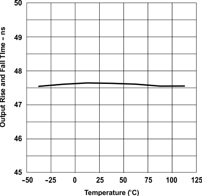
| tRISE | Rise tIme | TJ = 25°C, COUT = 1 nF | 25 | 50 | ns | |
| tFALL | Fall tIme | TJ = 25°C, COUT = 1 nF | 20 | 40 | ns | |
| UNDERVOLTAGE LOCKOUT | ||||||
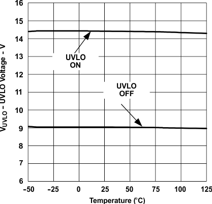
| VDDON | Start threshold(6) | UCC28C52-Q1, UCC28C54-Q1 | 13.5 | 14.5 | 15.5 | V |
| UCC28C53-Q1, UCC28C55-Q1 | 7.8 | 8.4 | 9 | |||
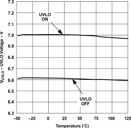
| UCC28C50-Q1, UCC28C51-Q1 | 6.5 | 7 | 7.5 | |||
UCC28C56H-Q1, UCC28C57H-Q1 | 17.6 | 18.8 | 20 | |||
| UCC28C56L-Q1, UCC28C57L-Q1 | 17.6 | 18.8 | 20 | |||
UCC28C58-Q1, UCC28C59-Q1 | 14.8 | 16 | 17.2 | |||
| VDDOFF | Minimum operating voltage (6) | UCC28C52-Q1, UCC28C54-Q1 | 8 | 9 | 10 | V |
| UCC28C53-Q1, UCC28C55-Q1 | 7 | 7.6 | 8.2 | |||
| UCC28C50-Q1, UCC28C51-Q1 | 6.1 | 6.6 | 7.1 | |||
| UCC28C56H-Q1, UCC28C57H-Q1 | 15 | 15.5 | 16 | |||
| UCC28C56L-Q1, UCC28C57L-Q1 | 13.95 | 14.5 | 15 | |||
| UCC28C58-Q1, UCC28C59-Q1 | 12 | 12.5 | 13 | |||
| VDDHyst | VDDON - VDDOFF(6) | UCC28C52-Q1, UCC28C54-Q1 | 5.4 | 5.5 | V | |
UCC28C53-Q1, UCC28C55-Q1 | 0.8 | 0.9 | ||||
UCC28C51-Q1, UCC28C50-Q1 | 0.4 | 0.5 | ||||
UCC28C56H-Q1, UCC28C57H-Q1 | 2.6 | 3.3 | ||||
UCC28C56L-Q1, UCC28C57L-Q1 | 3.65 | 4.3 | ||||
UCC28C58-Q1, UCC28C59-Q1 | 2.8 | 3.5 | ||||
| PWM | ||||||
| DMAX | Maximum duty cycle | UCC28C52-Q1, UCC28C53-Q1, UCC28C50-Q1, VFB < 2.4 V | 94% | 96% | ||
| UCC28C56H-Q1, UCC28C56L-Q1, UCC28C58-Q1, VFB < 2.4 V | ||||||
| UCC28C54-Q1, UCC28C55-Q1, UCC28C51-Q1, VFB < 2.4 V | 47% | 48% | ||||
| UCC28C57H-Q1, UCC28C57L-Q1, UCC28C59-Q1, VFB < 2.4 V | ||||||
| DMIN | Minimum duty cycle | VFB > 2.6 V | 0% | |||
| CURRENT SUPPLY | ||||||
| ISTART-UP | Start-up current | VVDD = VDDON – 0.5 V | 50 | 75 | µA | |
| IVDD | Operating supply current | VFB = VCS = 0 V | 1.3 | 2 | mA | |
7.6 Typical Characteristics
 Figure 7-1 Oscillator Frequency vs Timing Resistance and Capacitance
| Group 1: UCC28C50-Q1 to UCC28C55-Q1Group 2: UCC28C56H-Q1 to UCC28C59-Q1 |
| Group 1: UCC28C50-Q1 to UCC28C55-Q1Group 2: UCC28C56H-Q1 to UCC28C59-Q1 |
| UCC28C52-Q1 and UCC28C54-Q1 |
| UCC28C50-Q1 and UCC28C51-Q1 |
| UCC28C56L-Q1 and UCC28C57L-Q1 |
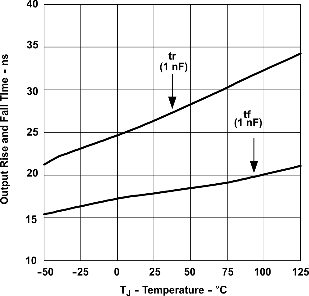 Figure 7-17 Output Rise Time and Fall Time vs Temperature
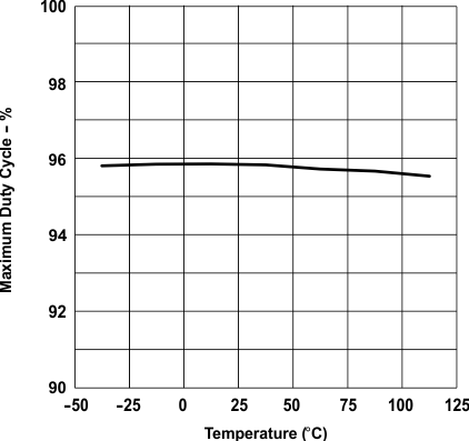
| UCC28C50-Q1, UCC28C52-Q1, UCC28C53-Q1, UCC28C56H/L-Q1, and UCC28C58-Q1 |
| Group 1: UCC28C50-Q1 to UCC28C55-Q1Group 2: UCC28C56H-Q1 to UCC28C59-Q1 |
| Group 1: UCC28C50-Q1 to UCC28C55-Q1Group 2: UCC28C56H-Q1 to UCC28C59-Q1 |
| VCS = 0Group 1: UCC28C50-Q1 to UCC28C55-Q1Group 2: UCC28C56H-Q1 to UCC28C59-Q1 |
| Group 1: UCC28C50-Q1 to UCC28C55-Q1Group 2: UCC28C56H-Q1 to UCC28C59-Q1 |
 Figure 7-8 Error Amplifier Input Bias Current vs Temperature
| UCC28C53-Q1 and UCC28C55-Q1 |
| UCC28C56H-Q1 and UCC28C57H-Q1 |
| UCC28C58-Q1 and UCC28C59-Q1 |
| Group 1: UCC28C50-Q1 to UCC28C55-Q1Group 2: UCC28C56H-Q1 to UCC28C59-Q1 |
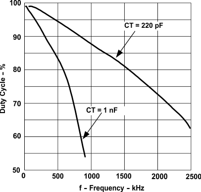 Figure 7-18 Maximum Duty Cycle vs Oscillator Frequency
| UCC28C51-Q1, UCC28C54-Q1, UCC28C55-Q1, UCC28C57H/L-Q1, and UCC28C59-Q1 |
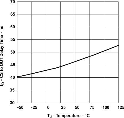 Figure 7-22 Current Sense to Output Delay Time vs Temperature
8 Detailed Description
8.1 Overview
The UCC28C5x-Q1 series of control integrated circuits provide the features necessary to implement AC-DC or DC‑to-DC fixed-frequency current-mode control schemes with a minimum number of external components. Protection circuitry includes undervoltage lockout (UVLO) and current limiting. Internally implemented circuits include a start-up current of less than 75 µA, a precision reference trimmed for accuracy at the error amplifier input, logic to ensure latched operation, a pulse-width modulation (PWM) comparator that also provides current-limit control, and an output stage designed to source or sink high-peak current. The output stage, suitable for driving N-channel MOSFETs, is low when it is in the OFF state. The oscillator contains a trimmed discharge current that enables accurate programming of the maximum duty cycle and dead time limit, making this device suitable for high-speed applications.
Major differences between members of this series are the UVLO thresholds, acceptable ambient temperature range, and maximum duty cycle and frequency. Typical UVLO thresholds of 14.5 V (ON) and 9 V (OFF) on the UCC28C52-Q1 and UCC28C54-Q1 devices make them ideally suited to off-line AC-DC applications. The corresponding typical thresholds for the UCC28C53-Q1 and UCC28C55-Q1 devices are 8.4-V (ON) and 7.6-V (OFF), making them ideal for use with regulated input voltages used in DC-DC applications. The UCC28C50-Q1 and UCC28C51-Q1 feature a start-up threshold of 7 V and a turnoff threshold of 6.6 V (OFF), which makes them suitable for battery- powered applications. The UCC28C56H/L-Q1, UCC28C57H/L-Q1, UCC28C58-Q1 and UCC28C59-Q1 operate with higher start-up thresholds for them suitably to work with SiC MOSFETs which often being used in high-voltage and high-power traction inverter applications. The UCC28C56H-Q1 and UCC28C57H-Q1 are with a start-up threshold 18.8-V (ON) and 15.5-V (OFF). The UCC28C56L-Q1 and UCC28C57L-Q1 are with a start-up threshold 18.8-V (ON) and 14.5-V (OFF). The UCC28C58-Q1 and UCC28C59-Q1 are with a start-up threshold 16-V (ON) and 12.5-V (OFF). The UCC28C50-Q1, UCC28C52-Q1, UCC28C53-Q1, UCC28C56H/L-Q1 and UCC28C58-Q1 devices operate to duty cycles approaching 100%. The UCC28C51-Q1, UCC28C54-Q1, UCC28C55-Q1, UCC28C57H/L-Q1 and UCC28C59-Q1 obtain a duty cycle from 0% to 50% by the addition of an internal toggle flip-flop, which blanks the output off every other clock cycle. The UCC28C5x series is specified for operation from –40°C to 125°C. The switching frequency (fSW) of the UCC28C50-Q1, UCC28C52-Q1, UCC28C53-Q1, UCC28C56H/L-Q1 and UCC28C58-Q1 gate drive is equal to fOSC; the switching frequency of the UCC28C51-Q1, UCC28C54-Q1, UCC28C55-Q1, UCC28C57H/L-Q1 and UCC28C59-Q1 is equal to half of the fOSC.
The UCC28C5x-Q1 series are an enhanced replacement with pin-to-pin compatibility to the BiCMOS UCC28C4x- Q1 families. The new series offers improved performance when compared to older bipolar devices and other competitive BiCMOS devices with similar functionality. These improvements generally consist of tighter specification limits that are a subset of the older product ratings, maintaining drop-in capability. In new designs, these improvements can reduce the component count or enhance circuit performance when compared to the previously available devices.