SBAS669A May 2014 – January 2015 ADC34J22 , ADC34J23 , ADC34J24 , ADC34J25
PRODUCTION DATA.
- 1 Features
- 2 Applications
- 3 Description
- 4 Revision History
- 5 Device Comparison Table
- 6 Pin Configuration and Functions
-
7 Specifications
- 7.1 Absolute Maximum Ratings
- 7.2 ESD Ratings
- 7.3 Recommended Operating Conditions
- 7.4 Summary of Special Mode Registers
- 7.5 Thermal Information
- 7.6 Electrical Characteristics: ADC34J24, ADC34J25
- 7.7 Electrical Characteristics: ADC34J22, ADC34J23
- 7.8 Electrical Characteristics: General
- 7.9 AC Performance: ADC34J25
- 7.10 AC Performance: ADC34J24
- 7.11 AC Performance: ADC34J23
- 7.12 AC Performance: ADC34J22
- 7.13 Digital Characteristics
- 7.14 Timing Characteristics
- 7.15 Typical Characteristics: ADC34J25
- 7.16 Typical Characteristics: ADC34J24
- 7.17 Typical Characteristics: ADC34J23
- 7.18 Typical Characteristics: ADC34J22
- 7.19 Typical Characteristics: Common Plots
- 7.20 Typical Characteristics: Contour Plots
- 8 Parameter Measurement Information
- 9 Detailed Description
- 10Application and Implementation
- 11Power-Supply Recommendations
- 12Layout
- 13Device and Documentation Support
- 14Mechanical, Packaging, and Orderable Information
Package Options
Mechanical Data (Package|Pins)
- RGZ|48
Thermal pad, mechanical data (Package|Pins)
- RGZ|48
Orderable Information
1 Features
- Quad Channel
- 12-Bit Resolution
- Single 1.8-V Supply
- Flexible Input Clock Buffer with Divide-by-1, -2, -4
- SNR = 69.6 dBFS, SFDR = 86 dBc at
fIN = 70 MHz - Ultra-Low Power Consumption:
- 203 mW/Ch at 160 MSPS
- Channel Isolation: 105 dB
- Internal Dither
- JESD204B Serial Interface:
- Subclass 0, 1, 2 Compliant up to 3.2 Gbps
- Supports One Lane per ADC up to 160 MSPS
- Support for Multi-Chip Synchronization
- Pin-to-Pin Compatible with 14-Bit Version
- Package: VQFN-48 (7 mm × 7 mm)
2 Applications
- Multi-Carrier, Multi-Mode Cellular Base Stations
- Radar and Smart Antenna Arrays
- Munitions Guidance
- Motor Control Feedback
- Network and Vector Analyzers
- Communications Test Equipment
- Nondestructive Testing
- Microwave Receivers
- Software Defined Radios (SDRs)
- Quadrature and Diversity Radio Receivers
3 Description
The ADC34J2x are a high-linearity, ultra-low power, dual-channel, 12-bit, 50-MSPS to 160-MSPS, analog-to-digital converter (ADC) family. The devices are designed specifically to support demanding, high input frequency signals with large dynamic range requirements. A clock input divider allows more flexibility for system clock architecture design while the SYSREF input enables complete system synchronization. The devices support JESD204B interfaces in order to reduce the number of interface lines, thus allowing for high system integration density. The JESD204B interface is a serial interface, where the data of each ADC are serialized and output over only one differential pair. An internal phase-locked loop (PLL) multiplies the incoming ADC sampling clock by 20 to derive the bit clock that is used to serialize the 12-bit data from each channel. The devices support subclass 1 with interface speeds up to 3.2 Gbps.
Device Information(1)
| PART NUMBER | PACKAGE | SAMPLING RATE (MSPS) |
|---|---|---|
| ADC34J22 | VQFN (48) | 50 |
| ADC34J23 | 80 | |
| ADC34J24 | 125 | |
| ADC34J25 | 160 |
- For all available packages, see the orderable addendum at the end of the datasheet.
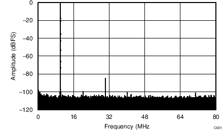
FFT with Dither On
(fS = 160 MSPS, fIN = 10 MHz, SNR = 70.3 dBFS, SFDR = 84 dBc)
4 Revision History
Changes from * Revision (May 2014) to A Revision
- Changed document status from product preview to production dataGo