SBAS788A January 2017 – August 2017 ADS7039-Q1
PRODUCTION DATA.
- 1 Features
- 2 Applications
- 3 Description
- 4 Revision History
- 5 Pin Configuration and Functions
- 6 Specifications
- 7 Parameter Measurement Information
- 8 Detailed Description
- 9 Application and Implementation
- 10Power Supply Recommendations
- 11Layout
- 12Device and Documentation Support
- 13Mechanical, Packaging, and Orderable Information
Package Options
Mechanical Data (Package|Pins)
- DCU|8
Thermal pad, mechanical data (Package|Pins)
Orderable Information
1 Features
- Qualified for Automotive Applications
- AEC-Q100 Qualified With the Following Results:
- Device Temperature Grade 1: –40°C to 125°C Ambient Operating Temperature Range
- Device HBM ESD Classification Level ±2000 V
- Device CDM ESD Classification Level ±1000 V
- Ultra-Low Power Consumption:
- 1.2 mW (max) at 2 MSPS with 3-V AVDD
- Less Than 1 µW at 1 kSPS with 3-V AVDD
- Miniature Footprint:
- 8-Pin VSSOP Package: 2.30 mm × 2.00 mm
- 2-MSPS Throughput with Zero Data Latency
- Wide Operating Range:
- AVDD: 2.35 V to 3.6 V
- DVDD: 1.65 V to 3.6 V (Independent of AVDD)
- Temperature Range: –40°C to +125°C
- Excellent Performance:
- 10-Bit Resolution with NMC
- ±0.4 LSB DNL; ±0.4 LSB INL
- 61-dB SNR with 3-V AVDD
- –75-dB THD with 3-V AVDD
- Unipolar Input Range: 0 V to AVDD
- Integrated Offset Calibration
- SPI-Compatible Serial Interface: 32 MHz
- JESD8-7A Compliant Digital I/O
2 Applications
- Automotive Infotainment
- Automotive Sensors
- Level Sensors
- Ultrasonic Flow Meters
- Motor Control
- Portable Medical Equipment
3 Description
The ADS7039-Q1 device is a an automotive Q100-qualified, 10-bit, 2-MSPS, analog-to-digital converter (ADC). The device supports a wide analog input voltage range (2.35 V to 3.6 V) and includes a capacitor-based, successive-approximation register (SAR) ADC with an inherent sample-and-hold circuit. The SPI-compatible serial interface is controlled by the CS and SCLK signals. The input signal is sampled with the CS falling edge and SCLK is used for conversion and serial data output. The device supports a wide digital supply range (1.65 V to 3.6 V), enabling direct interface to a variety of host controllers. The ADS7039-Q1 complies with the JESD8-7A standard for a normal DVDD range (1.65 V to 1.95 V).
The ADS7039-Q1 is available in an 8-pin, miniature, VSSOP package and is specified for operation from –40°C to +125°C. The fast sampling rate of the ADS7039-Q1, along with miniature form-factor and low-power consumption, makes this device suitable for space-constrained and fast-scanning automotive applications.
Device Information(1)
| PART NAME | PACKAGE | BODY SIZE (NOM) |
|---|---|---|
| ADS7039-Q1 | VSSOP (8) | 2.30 mm × 2.00 mm |
- For all available packages, see the orderable addendum at the end of the datasheet.
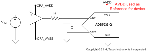
Typical Application
