SBAS676C November 2014 – December 2015 ADS7040
PRODUCTION DATA.
- 1 Features
- 2 Applications
- 3 Description
- 4 Revision History
- 5 Pin Configuration and Functions
- 6 Specifications
- 7 Parameter Measurement Information
- 8 Detailed Description
- 9 Application and Implementation
- 10Power-Supply Recommendations
- 11Layout
- 12Device and Documentation Support
- 13Mechanical, Packaging, and Orderable Information
Package Options
Refer to the PDF data sheet for device specific package drawings
Mechanical Data (Package|Pins)
- DCU|8
- RUG|8
Thermal pad, mechanical data (Package|Pins)
Orderable Information
1 Features
- Industry's First SAR ADC with Nanowatt Power Consumption:
- 171 µW at 1 MSPS with 1.8-V AVDD
- 555 µW at 1 MSPS with 3-V AVDD
- 56 µW at 100 kSPS with 3-V AVDD
- Less than 1 µW at 1 kSPS with 3-V AVDD
- Industry's Smallest SAR ADC:
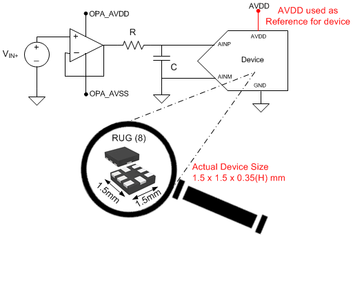
- X2QFN-8 Package with 2.25-mm2 Footprint
- 1-MSPS Throughput with Zero Data Latency
- Wide Operating Range:
- Excellent Performance:
- 8-Bit Resolution with NMC
- ±0.5-LSB (Max) INL, ±0.4-LSB (Max) DNL
- 49 dB SNR
- –70-dB THD
- Unipolar Input Range: 0 V to AVDD
- Integrated Offset Calibration
- SPI™-Compatible Serial Interface: 12 MHz
- JESD8-7A Compliant Digital I/O
2 Applications
- Low-Power Data Acquisition
- Battery-Powered Handheld Equipment
- Level Sensors
- Ultrasonic Flow Meters
- Motor Control
- Wearable Fitness
- Portable Medical Equipment
- Hard Drives
- Glucose Meters
3 Description
The ADS7040 is a 8-bit, 1-MSPS, analog-to-digital converter (ADC). The device supports a wide analog input voltage range (1.65 V to 3.6 V) and includes a capacitor-based, successive-approximation register (SAR) ADC with an inherent sample-and-hold circuit. The SPI-compatible serial interface is controlled by the CS and SCLK signals. The input signal is sampled with the CS falling edge and SCLK is used for conversion and serial data output. The device supports a wide digital supply range (1.65 V to 3.6 V), enabling direct interface to a variety of host controllers. The ADS7040 complies with the JESD8-7A standard for a normal DVDD range (1.65 V to
1.95 V).
The ADS7040 is available in 8-pin, miniature, leaded, and X2QFN packages and is specified for operation from –40°C to 125°C. Miniature form-factor and extremely low-power consumption make this device suitable for space-constrained, battery-powered applications.
Device Information(1)
| PART NAME | PACKAGE | BODY SIZE (NOM) |
|---|---|---|
| ADS7040 | X2QFN (8) | 1.50 mm × 1.50 mm |
| VSSOP (8) | 2.30 mm × 2.00 mm |
- For all available packages, see the orderable addendum at the end of the datasheet.
space
space
space
Typical Application
