SBAS677A June 2014 – October 2014 ADS8339
PRODUCTION DATA.
- 1 Features
- 2 Applications
- 3 Description
- 4 Revision History
- 5 Device Family
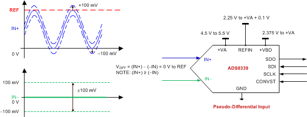
- 6 Pin Configuration and Functions
- 7 Specifications
- 8 Parametric Measurement Information
- 9 Detailed Description
- 10Application and Implementation
- 11Power-Supply Recommendations
- 12Layout
- 13Device and Documentation Support
- 14Mechanical, Packaging, and Orderable Information
Package Options
Mechanical Data (Package|Pins)
- DGS|10
Thermal pad, mechanical data (Package|Pins)
Orderable Information
1 Features
- Sample Rate: 250 kHz
- 16-Bit Resolution
- Zero Latency at Full Speed
- Unipolar Single-Ended Input Range:
- 0 V to Vref
- SPI™-Compatible Serial Interface with Daisy-Chain Option
- Uses Internal Clock for Conversion
- Excellent Performance:
- 93.6 dB SNR (typ) at 10-kHz Input
- –106 dB THD (typ) at 10-kHz Input
- ±2.0 LSB INL (max)
- ±1.0 LSB DNL (max)
- Low-Power Dissipation:
- 17.5 mW (typ) at 250 kSPS
- Power Scales Linearly with Speed:
- 1.75 mW at 25 kSPS
- Power Dissipation During Power-Down State:
- 0.25 μW (typ)
- Package: VSSOP-10
2 Applications
- Battery-Powered Equipment
- Data Acquisition Systems
- Instrumentation and Process Controls
- Medical Electronics
- Optical Networking
3 Description
The ADS8339 is a 16-bit, 250-kSPS, analog-to-digital converter (ADC). The device operates with a 2.25-V to 5.5-V external reference. The device includes a capacitor-based, successive-approximation register (SAR) ADC with an inherent sample-and-hold circuit.
The device includes a 25-MHz, SPI-compatible serial interface. The interface is designed to support daisy-chaining or cascading of multiple devices. Furthermore, a busy indicator makes synchronizing with the digital host easy. The unipolar, single-ended input range for the device supports an input swing of 0 V to Vref.
The device is optimized for low-power operation and power consumption scales directly with speed. This feature makes the device attractive for lower speed applications. The ADS8339 is available in a VSSOP-10 package.
Device Information(1)
| PART NUMBER | PACKAGE | BODY SIZE (NOM) |
|---|---|---|
| ADS8339 | VSSOP (10) | 3.00 mm × 3.00 mm |
- For all available packages, see the orderable addendum at the end of the datasheet.