SBAS619A March 2014 – June 2017 AFE5401-Q1
PRODUCTION DATA.
- 1 Features
- 2 Applications
- 3 Description
- 4 Revision History
- 5 Pin Configuration and Functions
-
6 Specifications
- 6.1 Absolute Maximum Ratings
- 6.2 ESD Ratings
- 6.3 Recommended Operating Conditions
- 6.4 Thermal Information
- 6.5 Electrical Characteristics
- 6.6 Digital Characteristics
- 6.7 Timing Requirements: Output Interface
- 6.8 Timing Requirements: RESET
- 6.9 Timing Requirements: Serial Interface Operation
- 6.10 Typical Characteristics
- 7 Parameter Measurement Information
- 8 Timing Requirements: Across Output Serialization Modes
-
9 Detailed Description
- 9.1 Overview
- 9.2 Functional Block Diagram
- 9.3 Feature Description
- 9.4 Device Functional Modes
- 9.5 Programming
- 9.6 Register Maps
- 10Application and Implementation
- 11Power Supply Recommendations
- 12Layout
- 13Device and Documentation Support
- 14Mechanical, Packaging, and Orderable Information
Package Options
Mechanical Data (Package|Pins)
- RGC|64
Thermal pad, mechanical data (Package|Pins)
- RGC|64
Orderable Information
1 Features
- Qualified for Automotive Applications
- AEC-Q100 Qualified With the Following Results:
- Device Temperature Grade 1: –40°C to 125°C Ambient Operating Temperature Range
- Device HBM ESD Classification Level 2
- Device CDM ESD Classification Level C4B
- Integrated Analog Front-End Includes:
- Input-Referred Noise with 30-dB PGA Gain:
- 2.9-nV/√Hz for 15-dB LNA Gain
- 2.0-nV/√Hz for 18-dB LNA Gain with HIGH_POW_LNA Mode
- Simultaneous Sampling Across Channels
- Programmable LNA Gain:
12 dB, 15 dB, 16.5 dB, and 18 dB - Programmable Equalizer Modes
- Built-In Diagnostic Modes
- Temperature Sensor
- Programmable-Gain Amplifiers (PGAs):
- 0 dB to 30 dB in 3-dB Steps
- Programmable, Third-Order, Antialiasing Filter:
- 7 MHz, 8 MHz, 10.5 MHz, and 12 MHz
- Analog-to-Digital Converter (ADC):
- Quad Channel, 12 Bits, 25 MSPS per Channel
- No External Decoupling Required for References
- Parallel CMOS Outputs
- 64-mW Total Core Power per Channel at
25 MSPS per Channel - Supplies: 1.8 V and 3.3 V
- Package: 9-mm × 9-mm VQFN-64
2 Applications
- Automotive Radar
- Data Acquisition
- SONAR™
3 Description
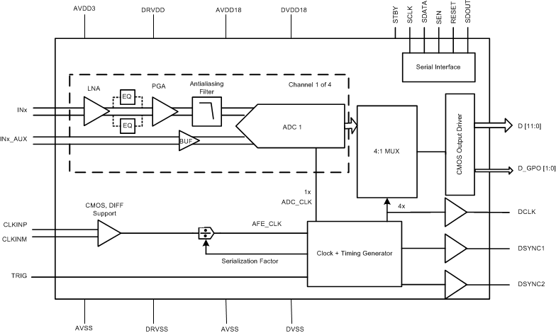
The AFE5401-Q1 is an analog front-end (AFE), targeting applications where the level of integration is critical. The device includes four channels, with each channel comprising a low-noise amplifier (LNA), a programmable equalizer (EQ), a programmable gain amplifier (PGA), and an antialias filter followed by a high-speed, 12-bit, analog-to-digital converter (ADC) at 25 MSPS per channel.
Each of the four differential input pairs are amplified by an LNA and are followed by a PGA with a programmable gain range from 0 dB to 30 dB. An antialias, low-pass filter (LPF) is also integrated between the PGA and ADC for each channel.
Each LNA, PGA, and antialiasing filter output is differential (limited to 2 VPP). The antialiasing filter drives the on-chip, 12-bit, 25-MSPS ADC. The four ADC outputs are multiplexed on a 12-bit, parallel, CMOS output bus.
The device is available in a 9-mm × 9-mm, VQFN-64 package and is specified over a temperature range of –40°C to +105°C. For more information, contact AFE5401_info@list.ti.com.
- For all available packages, see the orderable addendum at the end of the data sheet.
Simplified Schematic
