SLAS751D March 2011 – September 2015 DAC34H84
PRODUCTION DATA.
- 1 Features
- 2 Applications
- 3 Description
- 4 Revision History
- 5 Pin Configuration and Functions
-
6 Specifications
- 6.1 Absolute Maximum Ratings
- 6.2 ESD Ratings
- 6.3 Recommended Operating Conditions
- 6.4 Thermal Information
- 6.5 Electrical Characteristics - DC Specifications
- 6.6 Electrical Characteristics - Digital Specifications
- 6.7 Electrical Characteristics - AC Specifications
- 6.8 Timing Requirements - Digital Specifications
- 6.9 Switching Characteristics - AC Specifications
- 6.10 Typical Characteristics
-
7 Detailed Description
- 7.1 Overview
- 7.2 Functional Block Diagram
- 7.3
Feature Description
- 7.3.1 Serial Interface
- 7.3.2 Data Interface
- 7.3.3 Data Format
- 7.3.4 Input FIFO
- 7.3.5 FIFO Modes of Operation
- 7.3.6 Clocking Modes
- 7.3.7 FIR Filters
- 7.3.8 Complex Signal Mixer
- 7.3.9 Quadrature Modulation Correction (QMC)
- 7.3.10 Temperature Sensor
- 7.3.11 Data Pattern Checker
- 7.3.12 Parity Check Test
- 7.3.13 DAC34H84 Alarm Monitoring
- 7.3.14 LVPECL Inputs
- 7.3.15 LVDS Inputs
- 7.3.16 CMOS Digital Inputs
- 7.3.17 Reference Operation
- 7.3.18 DAC Transfer Function
- 7.3.19 Analog Current Outputs
- 7.4 Device Functional Modes
- 7.5 Programming
- 7.6 Register Map
- 8 Application and Implementation
- 9 Power Supply Recommendations
- 10Layout
- 11Device and Documentation Support
- 12Mechanical, Packaging, and Orderable Information
1 Features
- Very Low Power: 1.4 W at 1.25 GSPS
- Multi-DAC Synchronization
- Selectable 2x, 4x, 8x, 16x Interpolation Filter
- Stop-Band Attenuation > 90 dBc
- Flexible On-chip Complex Mixing
- Two Independent Fine Mixers with 32-bit NCOs
- Power Saving Coarse Mixers: ± n×Fs/8
- High Performance, Low Jitter Clock Multiplying PLL
- Digital I and Q Correction
- Gain, Phase, Offset, and Group Delay Correction
- Digital Inverse Sinc Filters
- 32-Bit DDR Flexible LVDS Input Data Bus
- 8 Sample Input FIFO
- Supports Data Rates up to 625 MSPS
- Data Pattern Checker
- Parity Check
- Temperature Sensor
- Differential Scalable Output: 10mA to 30mA
- 196-Ball, 12x12mm NFBGA (GREEN / Pb-Free)
2 Applications
- Cellular Base Stations
- Diversity Transmit
- Wideband Communications
3 Description
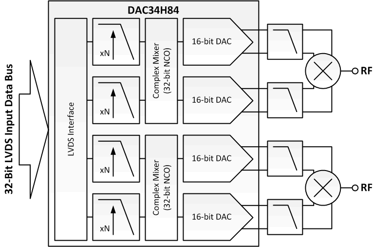
The DAC34H84 is a very low power, high dynamic range, quad-channel, 16-bit digital-to-analog converter (DAC) with a sample rate as high as 1.25 GSPS.
The device includes features that simplify the design of complex transmit architectures: 2x to 16x digital interpolation filters with over 90 dB of stop-band attenuation simplify the data interface and reconstruction filters. Independent complex mixers allow flexible carrier placement.
A high-performance low jitter clock multiplier simplifies clocking of the device without significant impact on the dynamic range. The digital Quadrature Modulator Correction (QMC) enables complete IQ compensation for gain, offset, phase and group delay between channels in direct up-conversion applications.
Digital data is input to the device through a 32-bit wide LVDS data bus with on-chip termination. The wide bus allows the processing of very high bandwidth signals. The device includes a FIFO, data pattern checker and parity test to ease the input interface. The interface also allows full synchronization of multiple devices.
The device is characterized for operation over the entire industrial temperature range of –40°C to 85°C and is available in a 196-ball, 12x12mm, 0.8mm pitch BGA package.
The DAC34H84 very low power, high bandwidth support, superior crosstalk, high dynamic range and features are an ideal fit for next generation communication systems.
Device Information(1)
| PART NUMBER | PACKAGE | BODY SIZE (NOM) |
|---|---|---|
| DAC34H84 | NFBGA (196) | 12.00 mm x 12.00 mm |
- For all available packages, see the orderable addendum at the end of the data sheet.
Simplified Schematic

4 Revision History
Changes from C Revision (August 2012) to D Revision
- Added ESD Ratings table, Feature Description section, Device Functional Modes, Application and Implementation section, Power Supply Recommendations section, Layout section, Device and Documentation Support section, and Mechanical, Packaging, and Orderable Information section. Go
Changes from B Revision (August 2011) to C Revision
- Added thermal information to the Absolute Maximum Ratings tableGo
- Added Recommended Operating Conditions tableGo
- Deleted TJ row from top of thermal tableGo
- Deleted OPERATING RANGE section from bottom of Electrical Characteristics – DC SpecificationsGo
Changes from A Revision (June 2011) to B Revision
- Changed ALARM descriptionGo
- Added notes to Electrical Characteristics – DC SpecificationsGo
- Deleted t(align) from Electrical Characteristics – Digital SpecificationsGo
- Added fDAC PLL ON MIN of 1000 MSPS in Electrical Characteristics – AC SpecificationsGo
- Changed DIGITAL INPUT TIMING SPECIFICATIONS in Timing Requirements - Digital SpecificationsGo
- Changed DAC Wake-up Time in Switching Characteristics – AC SpecificationsGo
- Added information to SINGLE SYNC SOURCE MODE sectionGo
- Deleted t(align) from BYPASS MODE sectionGo
- Changed 1.2288GHz to 983.04MHz in PLL MODE descriptionGo
- Changed data in Table 4Go
- Deleted 2x in Table 6Go
- Changed EXAMPLE START-UP ROUTINE informationGo
- Changed Table 10Go
- Changed register version default value from 0x5408 to 0x5409 in Register MapGo
- Deleted t(align) from register config0 descriptionGo
- Added SIF SYNC to register config32 descriptionGo
- Changed B40 to N11 in register config35 descriptionGo
- Changed register config 45 default valueGo
- Changed register version default value from 0x5408 to 0x5409Go
Changes from * Revision (March 2011) to A Revision
- Changed from PRODUCT PREVIEW to PRODUCTION DATAGo