DATA SHEET
LM10011 用于负载点稳压器且具有可调节启动电流的 6/4 位 VID 可编程电流 DAC
本资源的原文使用英文撰写。 为方便起见,TI 提供了译文;由于翻译过程中可能使用了自动化工具,TI 不保证译文的准确性。 为确认准确性,请务必访问 ti.com 参考最新的英文版本(控制文档)。
1 特性
2 应用
- 宽带、网络互联及无线通信
- 笔记本电源解决方案
- 便携式仪器
- 电池供电类设备
- 为具有 6 位或 4 位 4 引脚 VID 接口的数字负载供电
3 说明
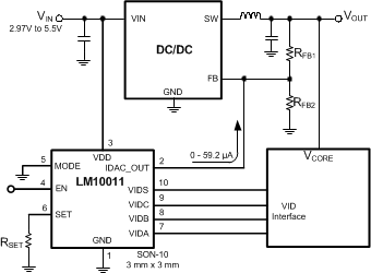
LM10011 是一款用于控制直流/直流 (DC/DC) 转换器输出电压的精密数字可编程器件。 LM10011 输出的直流电流与 6 位或 4 位输入字成正比。 通过将 IDAC_OUT 引脚连接至稳压器的反馈节点,可以将稳压器输出电压调整为用户设置的范围和分辨率。 随着输入字递增计数,根据转换器中反馈电阻的值适当调高输出电压。
可通过外部电阻来编程 IDAC_OUT 引脚的启动电流,以覆盖 0 至 56.4µA 电流范围(分辨率为 4 位)。 MODE 引脚允许通过 4 位并行 VID 接口或 6 位接口(包含高 3 位和低 3 位 VID 代码)对器件进行编程。 LM10011 专用于针对 VID(电压识别)应用编程各类德州仪器 (TI) DC/DC 转换器。
器件信息(1)
| 器件型号 | 封装 | 封装尺寸(标称值) |
|---|---|---|
| LM10011 | WSON (10) | 3.00mm x 3.00mm |
- 要了解所有可用封装,请见数据表末尾的可订购产品附录。
典型应用电路
4 修订历史记录
Changes from * Revision (December 2012) to A Revision
- Added 引脚配置和功能部分,处理额定值表,特性描述部分,器件功能模式,应用和实施部分,电源相关建议部分,布局部分,器件和文档支持部分以及机械、封装和可订购信息部分Go
5 Pin Configuration and Functions
10-PIN
WSON PACKAGE
TOP VIEW
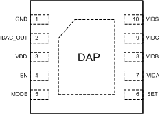
Pin Functions
| PIN | I/O | DESCRIPTION | |
|---|---|---|---|
| NAME | NUMBER | ||
| GND | 1 | – | Ground |
| IDAC_OUT | 2 | O | Output pin of the current DAC that connects to the feedback node of the regulator. |
| VDD | 3 | I | Positive supply input. Operating voltage is 2.97 V to 5.5 V. It is recommended to add a small 1-nF or greater bypass capacitor from this pin to GND. |
| EN | 4 | I | Precision enable input. The LM10011 will operate when the EN pin voltage exceeds 1.34 V. |
| MODE | 5 | – | MODE will set the VID operating mode. Connecting MODE to VDD will select a 4-bit parallel interface. Connecting MODE to GND will select a 4-pin, 6-bit interface. |
| SET | 6 | – | A resistor connected from SET to GND will set the start-up code (current) at the IDAC_OUT pin. There are 16 different start-up codes to select from. |
| VIDA | 7 | I | VID digital input. In 6-bit mode: Bit 0 when VIDS transitions low; Bit 3 when VIDS transitions high. In 4-bit mode: Bit 0. |
| VIDB | 8 | I | VID digital input. In 6-bit mode: Bit 1 when VIDS transitions low; Bit 4 when VIDS transitions high. In 4-bit mode: Bit 1. |
| VIDC | 9 | I | VID digital input. In 6-bit mode: Bit 2 when VIDS transitions low; Bit 5 when VIDS transitions high. In 4-bit mode: Bit 2. |
| VIDS | 10 | I | VID select line. In 6-bit mode: transition low selects lower 3 bits, transition high selects upper 3 bits and updates the IDAC_OUT current to reflect the present VID code. In 4-bit mode: Bit 3. |
| DAP | DAP | – | Die Attach Pad. Not electrically connected to device, connect to system ground plane for reduced thermal resistance. |
6 Specifications
6.1 Absolute Maximum Ratings(1)(2)
over operating free-air temperature range (unless otherwise noted)| MIN | MAX | UNIT | ||
|---|---|---|---|---|
| VDD, EN, IDAC_OUT, MODE | –0.3 | 6 | V | |
| VIDA, VIDB, VIDC, VIDS | –0.3 | 6 | V | |
| Junction Temperature | 150 | °C | ||
(1) Absolute Maximum Ratings indicate limits beyond which damage to the device may occur.
(2) If Military- or Aerospace-specified devices are required, please contact the Texas Instruments Sales Office / Distributors for availability and specifications.
6.2 Handling Ratings
| MIN | MAX | UNIT | |||
|---|---|---|---|---|---|
| Tstg | Storage temperature range | –65 | 150 | °C | |
| V(ESD) | Electrostatic discharge | Human body model (HBM), per ANSI/ESDA/JEDEC JS-001, all pins(1) | 2 | kV | |
| Charged device model (CDM), per JEDEC specification JESD22-C101, all pins(2) | 1 | ||||
(1) JEDEC document JEP155 states that 500-V HBM allows safe manufacturing with a standard ESD control process.
(2) JEDEC document JEP157 states that 250-V CDM allows safe manufacturing with a standard ESD control process.
6.3 Recommended Operating Conditions
over operating free-air temperature range (unless otherwise noted)| MIN | MAX | UNIT | ||
|---|---|---|---|---|
| VDD | 2.97 | 5.5 | V | |
| IDAC_OUT | –0.3 | VDD – 1.75 | V | |
| VIDA, VIDB, VIDC, VIDS, EN, MODE | –0.3 | 5.5 | V | |
| Junction Temperature | −40 | 125 | °C | |
| Ambient Temperature | −40 | 125 | °C | |
6.4 Thermal Information
| THERMAL METRIC(1) | LM10011 | UNIT | |
|---|---|---|---|
| DSC | |||
| 10 PINS | |||
| RθJA | Junction-to-ambient thermal resistance(2) | 52.1 | °C/W |
| RθJC(top) | Junction-to-case (top) thermal resistance(3) | 30.6 | |
| RθJB | Junction-to-board thermal resistance(4) | 26.8 | |
| ψJT | Junction-to-top characterization parameter(5) | 0.9 | |
| ψJB | Junction-to-board characterization parameter(6) | 26.9 | |
| RθJC(bot) | Junction-to-case (bottom) thermal resistance(7) | 7.7 | |
(1) For more information about traditional and new thermal metrics, see the IC Package Thermal Metrics application report, SPRA953.
(2) The junction-to-ambient thermal resistance under natural convection is obtained in a simulation on a JEDEC-standard, high-K board, as specified in JESD51-7, in an environment described in JESD51-2a.
(3) The junction-to-case (top) thermal resistance is obtained by simulating a cold plate test on the package top. No specific JEDEC-standard test exists, but a close description can be found in the ANSI SEMI standard G30-88.
(4) The junction-to-board thermal resistance is obtained by simulating in an environment with a ring cold plate fixture to control the PCB temperature, as described in JESD51-8.
(5) The junction-to-top characterization parameter, ψJT, estimates the junction temperature of a device in a real system and is extracted from the simulation data for obtaining RθJA, using a procedure described in JESD51-2a (sections 6 and 7).
(6) The junction-to-board characterization parameter, ψJB, estimates the junction temperature of a device in a real system and is extracted from the simulation data for obtaining RθJA, using a procedure described in JESD51-2a (sections 6 and 7).
(7) The junction-to-case (bottom) thermal resistance is obtained by simulating a cold plate test on the exposed (power) pad. No specific JEDEC standard test exists, but a close description can be found in the ANSI SEMI standard G30-88.
6.5 Electrical Characteristics
Typical values correspond to TJ = 25°C. Minimum and maximum limits apply over –40°C to 125°C junction temperature range unless otherwise stated.(4)(5)| PARAMETER | TEST CONDITIONS | MIN | TYP | MAX | UNIT | |
|---|---|---|---|---|---|---|
| SUPPLY, UVLO, AND ENABLE | ||||||
| IQ | Quiescent current | VDD = 5.0 V, VEN = 2.0 V | 260 | 300 | µA | |
| IQ_FS | Quiescent current, IDAC_OUT = IFS_6 | VDD = 5.0 V, VEN = 2.0 V, IFS_6 | 382 | µA | ||
| IQ_DIS | Quiescent current disabled | VDD = 5.0 V, VEN = 0.0 V | 45 | 65 | µA | |
| VUVLO_R | Undervoltage rising threshold | VDD rising | 2.65 | 2.95 | V | |
| VUVLO_F | Undervoltage falling threshold | VDD falling | 2.2 | 2.45 | V | |
| VUVLO_HYS | Hysteresis | 200 | mV | |||
| VEN | Enable rising threshold | VEN rising | 1.20 | 1.34 | 1.45 | V |
| VEN_HYS | Enable hysteresis | 50 | 100 | 180 | mV | |
| IEN | Enable pullup current | 2 | µA | |||
| IDAC_OUT | ||||||
| ACC | Accuracy | Measured at full scale | –1.25 | 1.25 | % | |
| ACC | Accuracy | Measured at full scale, 0°C to 100°C | –1.0 | 1.0 | % | |
| LSB_6 | DAC step size, 6-bit mode | IFS_6 / (26 – 1) | 940 | nA | ||
| LSB_4 | DAC step size, 4-bit mode | IFS_4 / (24 – 1) | 3.76 | µA | ||
| IFS_6 | Full-scale output current (6-bit mode) | VID[5:0] = 000000b | 59.2 | µA | ||
| IFS_4 | Full-scale output current (4-bit mode) | VID[3:0] = 0000b | 56.4 | µA | ||
| INL | Integral non-linearity | –1 | 1 | LSB_6 | ||
| DNL | Differential non-linearity | –0.25 | 0.25 | LSB_6 | ||
| OFFSET | Offset current | VID[5:0] = 111111b (6-bit), VID[3:0] = 1111b (4-bit) | 60 | nA | ||
| VOUT_MAX | IDAC_OUT compliance voltage | VDD = 3 V, VDD-VIDAC_OUT | 1.75 | V | ||
| START-UP SET CURRENT | ||||||
| VSETFSR | SET pin voltage FSR | 1.12 | 1.2 | 1.23 | V | |
| SETRES | SET ADC resolution | 4 | bits | |||
| SETRNG | SET ADC current full-scale range | 56.4 | µA | |||
| ISET | SET Current | 4.75 | 5.1 | 5.40 | µA | |
| SET0 | Start-up DAC error, code 0 | RSET = 0 Ω, IDAC_OUT = 56.4 µA | 0 | 0 | LSB | |
| SET1 | Start-up DAC error, code 1 | RSET = 21.0 kΩ(2), IDAC_OUT = 52.7 µA | 0 | 0 | LSB | |
| SET2 | Start-up DAC error, code 2 | RSET = 35.7 kΩ(2), IDAC_OUT = 48.9 µA | 0 | 0 | LSB | |
| SET3 | Start-up DAC error, code 3 | RSET = 51.1 kΩ(2), IDAC_OUT = 45.2 µA | 0 | 0 | LSB | |
| SET4 | Start-up DAC error, code 4(1) | RSET = 71.5 kΩ(2), IDAC_OUT = 41.4 µA | 0 | 1 | LSB | |
| SET5 | Start-up DAC error, code 5(1) | RSET = 86.6 kΩ(2), IDAC_OUT = 37.7 µA | 0 | 1 | LSB | |
| SET6 | Start-up DAC error, code 6(1) | RSET = 105 kΩ(2), IDAC_OUT = 33.9 µA | 0 | 1 | LSB | |
| SET7 | Start-up DAC error, code 7(1) | RSET = 118 kΩ(2), IDAC_OUT = 30.1 µA | 0 | 1 | LSB | |
| SET8 | Start-up DAC error, code 8(1) | RSET = 140 kΩ(2), IDAC_OUT =26.4 µA | 0 | 1 | LSB | |
| SET9 | Start-up DAC error, code 9(1) | RSET = 154 kΩ(2), IDAC_OUT = 22.6 µA | 0 | 1 | LSB | |
| SET10 | Start-up DAC error, code 10(1) | RSET = 169 kΩ(2), IDAC_OUT = 18.8 µA | 0 | 1 | LSB | |
| SET11 | Start-up DAC error, code 11(1) | RSET = 182 kΩ(2), IDAC_OUT = 15.1 µA | 0 | 1 | LSB | |
| SET12 | Start-up DAC error, code 12(1) | RSET = 200 kΩ(2), IDAC_OUT = 11.3 µA | 0 | 1 | LSB | |
| SET13 | Start-up DAC error, code 13(1) | RSET = 215 kΩ(2), IDAC_OUT = 7.59 µA | 0 | 1 | LSB | |
| SET14 | Start-up DAC error, code 14(1) | RSET = 237 kΩ(2), IDAC_OUT = 3.80 µA | 0 | 1 | LSB | |
| SET15 | Start-up DAC error, code 15 | RSET = 301 kΩ(2), IDAC_OUT = 0.06 µA | 0 | 0 | LSB | |
| VID LOGIC INPUTS(3) | ||||||
| VIL | Input voltage low | 0.75 | V | |||
| VIH | Input voltage high | 1.0 | V | |||
| IIL | Input current low | –3.5 | µA | |||
| IIH | Input current high | 5 | µA | |||
| tDEGLITCH | Input deglitch time | 3.6 | µs | |||
| t1 | Input delay time | VIDS rising edge | 1 | µs | ||
| t2 | Input hold time VIDA, VIDB, VIDC valid | VIDS falling edge | 20 | µs | ||
| t3 | Input delay time | VIDS falling edge | 1 | µs | ||
| t4 | Input hold time VIDA, VIDB, VIDC valid | VIDS rising edge | 20 | µs | ||
| t5 | Delay to beginning of IDAC_OUT transition | Measured from VIDS rising edge | 6.3 | 10 | µs | |
| t6 | IDAC_OUT transition time | Time constant for exponential rise | 40 | µs | ||
| t7 | Minimum hold time in 4-bit mode | VIDA, VIDB, VIDC, VIDS | 4.4 | µs | ||
(1) "+1" LSB implies a positive step in CODE. LSB is in reference to LSB_4.
(2) RSET is based on 1% E96 standard resistor values.
(3) For VID timing, see Figure 1.
(4) All hot and cold limits are specified by correlating the electrical characteristics to process and temperature variations and applying statistical process control.
(5) The junction temperature (TJ in °C) is calculated from the ambient temperature (TA in °C) and power dissipation (PD in Watts) as follows: TJ = TA + (PD × RθJA) where RθJA (in °C/W) is the package thermal impedance provided in the Thermal Information section.
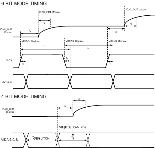 Figure 1. Timing Diagram for LM10011 Communications
6.6 Typical Characteristics
Unless otherwise specified, the following conditions apply: TJ = 25°C, VDD = 5 V. All graphs show junction temperature.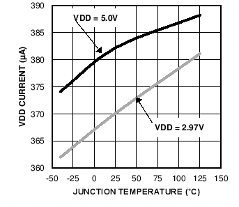 Figure 2. Supply Current
Maximum Output Current VID = [000000]
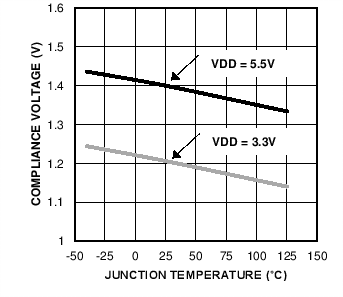 Figure 4. Output Compliance to Positive Rail
 (VDD-VIDAC_OUT)
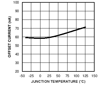 Figure 6. IDAC_OUT Offset Current
VID = [111111]
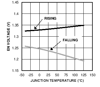 Figure 8. Enable (EN) Threshold
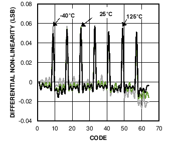 Figure 10. Differential Non-Linearity
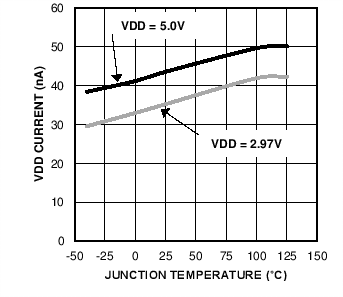 Figure 3. Supply Current (EN LOW)
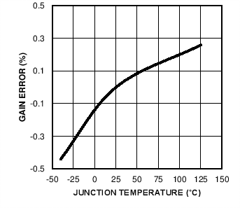 Figure 5. Gain Error
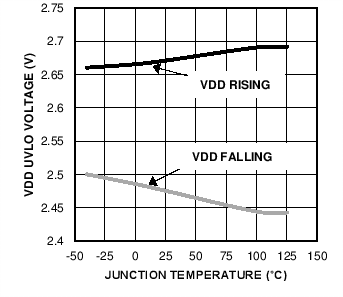 Figure 7. UVLO Thresholds
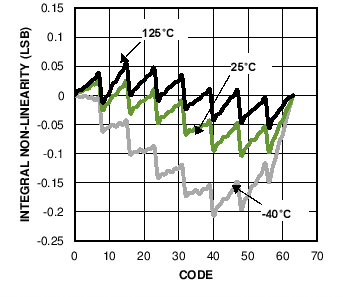 Figure 9. Integral Non-Linearity