SNVS764Q January 2000 – December 2017 LP2950-N , LP2951-N
PRODUCTION DATA.
- 1 Features
- 2 Applications
- 3 Description
- 4 Revision History
- 5 Voltage Options
- 6 Pin Configuration and Functions
- 7 Specifications
-
8 Detailed Description
- 8.1 Overview
- 8.2 Functional Block Diagrams
- 8.3 Feature Description
- 8.4 Device Functional Modes
-
9 Application and Implementation
- 9.1 Application Information
- 9.2
Typical Applications
- 9.2.1 1-A Regulator with 1.2-V Dropout
- 9.2.2 300-mA Regulator with 0.75-V Dropout
- 9.2.3 Wide Input Voltage Range Current Limiter
- 9.2.4 Low Drift Current Source
- 9.2.5 5-V Current Limiter
- 9.2.6 Regulator with Early Warning and Auxiliary Output
- 9.2.7 Latch Off When Error Flag Occurs
- 9.2.8 2-A Low Dropout Regulator
- 9.2.9 5-V Regulator with 2.5-V Sleep Function
- 9.2.10 Open Circuit Detector for 4 → 20-mA Current Loop
- 9.2.11 Regulator with State-of-Charge Indicator
- 9.2.12 Low Battery Disconnect
- 9.2.13 System Overtemperature Protection Circuit
- 10Power Supply Recommendations
- 11Layout
- 12Device and Documentation Support
- 13Mechanical, Packaging, and Orderable Information
封装选项
机械数据 (封装 | 引脚)
散热焊盘机械数据 (封装 | 引脚)
订购信息
1 Features
- Input Voltage Range: 2.3 V to 30 V
- 5-V, 3-V, and 3.3-V Output Voltage Versions Available
- High Accuracy Output Voltage
- Ensured 100-mA Output Current
- Extremely Low Quiescent Current
- Low Dropout Voltage
- Extremely Tight Load and Line Regulation
- Very Low Temperature Coefficient
- Use as Regulator or Reference
- Needs Minimum Capacitance for Stability
- Current and Thermal Limiting
- Stable With Low-ESR Output Capacitors (10 mΩ to 6 Ω)
- LP2951-N Versions Only:
- Error Flag Warns of Output Dropout
- Logic-Controlled Electronic Shutdown
- Output Programmable From 1.24 V to 29 V
2 Applications
- High-Efficiency Linear Regulator
- Regulator with Undervoltage Shutdown
- Low Dropout Battery-powered Regulator
- Snap-ON/Snap-OFF Regulator
space
space
space
space
space
space
space
space
space
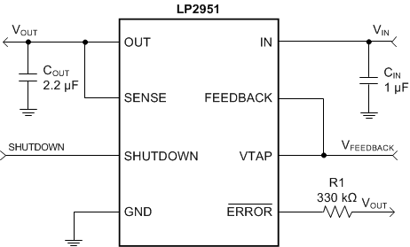
LP2951 Simplified Schematic

3 Description
The LP2950-N and LP2951-N are micropower voltage regulators with very low quiescent current (75 µA typical) and very low dropout voltage (typical 40 mV at light loads and 380 mV at 100 mA). They are ideally suited for use in battery-powered systems. Furthermore, the quiescent current of the device increases only slightly in dropout, prolonging battery life.
Careful design of the LP2950-N/LP2951-N has minimized all contributions to the error budget. This includes a tight initial tolerance (0.5% typical), extremely good load and line regulation (0.05% typical) and a very low output voltage temperature coefficient, making the part useful as a low-power voltage reference.
One such feature is an error flag output which warns of a low output voltage, often due to falling batteries on the input. It may be used for a power-on reset. A second feature is the logic-compatible shutdown input which enables the regulator to be switched on and off. Also, the part may be pin-strapped for a 5-V, 3-V, or 3.3-V output (depending on the version), or programmed from 1.24 V to 29 V with an external pair of resistors.
The LP2950-N is available in the surface-mount TO-252 package and in the popular 3-pin TO-92 package for pin-compatibility with older 5-V regulators. The 8-pin LP2951-N is available in plastic, ceramic dual-in-line, WSON, or metal can packages and offers additional system functions.
Device Information(1)
| PART NUMBER | PACKAGE | BODY SIZE (NOM) |
|---|---|---|
| LP2950-N | TO-92 (3) | 4.30 mm × 4.30 mm |
| TO-252 (3) | 9.91 mm × 6.58 mm | |
| LP2951-N | SOIC (8) | 4.90 mm × 3.91 mm |
| VSSOP (8) | 3.00 mm × 3.00 mm | |
| WSON (8) | 4.00 mm × 4.00 mm | |
| PDIP (8) | 9.81 mm × 6.35 mm |
- For all available packages, see the orderable addendum at the end of the data sheet.
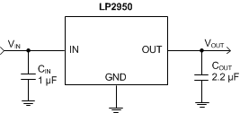
LP2950-N Simplified Schematic

4 Revision History
Changes from P Revision (May 2016) to Q Revision
- Changed LP2951-N ESD parameter pin references and added SENSE pin row to LP2951-N ESD parameter in ESD Ratings tableGo
Changes from O Revision (December 2014) to P Revision
- Added rows to ESD Ratings table to differentiate values for pins 3 and 7 of the LP2951-N deviceGo
- Added footnotes 2 and 3 to both Thermal Information tables Go
Changes from N Revision (May 2013) to O Revision
- Added Device Information and ESD Rating tables, Feature Description, Device Functional Modes, Application and Implementation, Power Supply Recommendations, Layout, Device and Documentation Support, and Mechanical, Packaging, and Orderable Information sections; moved some curves to Application Curves section; update pin names; change package nomenclature from National to TI Go
Changes from M Revision (April 2013) to N Revision
- Changed layout of National Data Sheet to TI format Go