SCES204Q April 1999 – March 2017 SN74LVC2G125
PRODUCTION DATA.
- 1 Features
- 2 Applications
- 3 Description
- 4 Revision History
- 5 Pin Configuration and Functions
- 6 Specifications
- 7 Parameter Measurement Information
- 8 Detailed Description
- 9 Application and Implementation
- 10Power Supply Recommendations
- 11Layout
- 12Device and Documentation Support
- 13Mechanical, Packaging, and Orderable Information
封装选项
请参考 PDF 数据表获取器件具体的封装图。
机械数据 (封装 | 引脚)
- DCU|8
- YZP|8
- DCT|8
散热焊盘机械数据 (封装 | 引脚)
订购信息
1 Features
- ESD Protection Exceeds JESD 22
- 2000-V Human-Body Model
- 1000-V Charged-Device Model
- Available in the Texas Instruments
NanoFree™ Package - Supports 5-V VCC Operation
- Inputs Accept Voltages to 5.5 V
- Max tpd of 4.3 ns at 3.3 V
- Low Power Consumption, 10-µA Max ICC
- ±24-mA Output Drive at 3.3 V
- Typical VOLP (Output Ground Bounce)
< 0.8 V at VCC = 3.3 V, TA = 25°C - Typical VOHV (Output VOH Undershoot)
> 2 V at VCC = 3.3 V, TA = 25°C - Ioff Supports Live Insertion, Partial-Power-Down Mode, and Back-Drive Protection
- Can Be Used as a Down Translator to Translate Inputs From a Max of 5.5 V Down
to the VCC Level - Latch-Up Performance Exceeds 100 mA Per
JESD 78, Class II
2 Applications
- Cable Modem Termination Systems
- High-Speed Data Acquisition and Generation
- Military: Radars and Sonars
- Motor Controls: High-Voltage
- Power Line Communication Modems
- SSDs: Internal or External
- Video Broadcasting and Infrastructure: Scalable Platforms
- Video Broadcasting: IP-Based Multi-Format Transcoders
- Video Communications Systems
3 Description
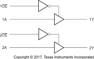
The SN74LVC2G125 device is a dual bus buffer gate, designed for 1.65-V to 5.5-V VCC operation. This device features dual line drivers with 3-state outputs. The outputs are disabled when the associated output-enable (OE) input is high.
NanoFree™ package technology is a major breakthrough in IC packaging concepts, using the die as the package.
To ensure the high-impedance state during power up or power down, OE should be tied to VCC through a pullup resistor; the minimum value of the resistor is determined by the current-sinking capability of the driver.
This device is fully specified for partial-power-down applications using Ioff. The Ioff circuitry disables the outputs, preventing damaging current backflow through the device when it is powered down.
Device Information(1)
| PART NUMBER | PACKAGE | BODY SIZE |
|---|---|---|
| SN74LVC2G125DCTR | SM8 (8) | 2.95 mm × 2.80 mm |
| SN74LVC2G125DCUR | VSSOP (8) | 2.30 mm × 2.00 mm |
| SN74LVC2G125YZPR | DSBGA (8) | 1.91 mm × 0.91 mm |
- For all available packages, see the orderable addendum at the end of the data sheet.
