SLVS568D January 2005 – April 2016 TLV341 , TLV341A , TLV342 , TLV342S
PRODUCTION DATA.
- 1 Features
- 2 Applications
- 3 Description
- 4 Revision History
- 5 Pin Configuration and Functions
-
6 Specifications
- 6.1 Absolute Maximum Ratings
- 6.2 ESD Ratings
- 6.3 Recommended Operating Conditions
- 6.4 Thermal Information: TLV341
- 6.5 Thermal Information: TLV342
- 6.6 Thermal Information: TLV342S
- 6.7 Electrical Characteristics: V+ = 1.8 V
- 6.8 Electrical Characteristics: V+ = 5 V
- 6.9 Shutdown Characteristics: V+ = 1.8 V
- 6.10 Shutdown Characteristics: V+ = 5 V
- 6.11 Typical Characteristics
- 7 Detailed Description
- 8 Application and Implementation
- 9 Power Supply Recommendations
- 10Layout
- 11Device and Documentation Support
- 12Mechanical, Packaging, and Orderable Information
1 Features
- 1.8-V and 5-V Performance
- Low Offset (A Grade)
- 1.25 mV Maximum (25°C)
- 1.7 mV Maximum (–40°C to 125°C)
- Rail-to-Rail Output Swing
- Wide Common-Mode Input Voltage Range: –0.2 V to (V+ – 0.5 V)
- Input Bias Current: 1 pA (Typical)
- Input Offset Voltage: 0.3 mV (Typical)
- Low Supply Current: 70 μA/Channel
- Low Shutdown Current:
10 pA (Typical) Per Channel - Gain Bandwidth: 2.3 MHz (Typical)
- Slew Rate: 0.9 V/μs (Typical)
- Turnon Time From Shutdown: 5 μs (Typical)
- Input Referred Voltage Noise (at 10 kHz):
20 nV/√Hz - ESD Protection Exceeds JESD 22
- 2000-V Human-Body Model (HBM)
- 750-V Charged-device model (CDM)
2 Applications
3 Description
The TLV34xx devices are single and dual CMOS operational amplifiers, respectively, with low-voltage, low-power, and rail-to-rail output swing capabilities. The PMOS input stage offers an ultra-low input bias current of 1 pA (typical) and an offset voltage of
0.3 mV (typical). For applications requiring excellent dc precision, the A grade (TLV34xA) has a low offset voltage of 1.25 mV (maximum) at 25°C.
These single-supply amplifiers are designed specifically for ultra-low-voltage (1.5 V to 5 V) operation, with a common-mode input voltage range that typically extends from –0.2 V to 0.5 V from the positive supply rail.
The TLV341 (single) and TLV342 (dual) in the RUG package also offer a shutdown (SHDN) pin that can be used to disable the device. In shutdown mode, the supply current is reduced to 45 pA (typical). Offered in both the SOT-23 and smaller SC70 packages, the TLV341 is suitable for the most space-constrained applications. The dual TLV342 is offered in the standard SOIC, VSSOP, and X2QFN packages.
An extended industrial temperature range from –40°C to 125°C makes the TLV34xx suitable in a wide variety of commercial and industrial applications.
Device Information(1)
| PART NUMBER | PACKAGE | BODY SIZE (NOM) |
|---|---|---|
| TLV341 | SOT-23 (6) | 2.90 mm × 1.60 mm |
| SC70 (6) | 2.00 mm × 1.25 mm | |
| SOT (6) | 1.60 mm × 1.20 mm | |
| TLV342 | SOIC (8) | 4.90 mm × 3.91 mm |
| VSSOP (8) | 3.00 mm × 3.00 mm | |
| X2QFN (10) | 1.50 mm × 2.00 mm | |
| TLV342S | X2QFN (10) | 1.50 mm × 2.00 mm |
- For all available packages, see the orderable addendum at the end of the data sheet.
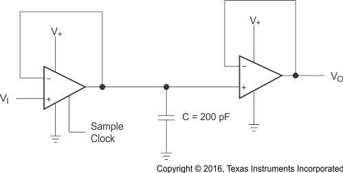
Sample and Hold Circuit Using Two TLV341
