SLOS369G July 2002 – October 2015 TPA2005D1
PRODUCTION DATA.
- 1 Features
- 2 Applications
- 3 Description
- 4 Revision History
- 5 Device Comparison Table
- 6 Pin Configuration and Functions
- 7 Specifications
- 8 Parameter Measurement Information
- 9 Detailed Description
- 10Application and Implementation
- 11Power Supply Recommendations
- 12Layout
- 13Device and Documentation Support
- 14Mechanical, Packaging, and Orderable Information
封装选项
请参考 PDF 数据表获取器件具体的封装图。
机械数据 (封装 | 引脚)
- DGN|8
- DRB|8
散热焊盘机械数据 (封装 | 引脚)
订购信息
1 Features
- 1.4 W Into 8 Ω From a 5 V Supply at
THD = 10% (Typ) - Maximum Battery Life and Minimum Heat
- Efficiency With an 8-Ω Speaker:
- 84% at 400 mW
- 79% at 100 mW
- 2.8-mA Quiescent Current
- 0.5-μA Shutdown Current
- Efficiency With an 8-Ω Speaker:
- Capable of Driving an
8-Ω Speaker (2.5 V ≤ VDD ≤ 5.5 V) and a
4-Ω Speaker (2.5 V ≤ VDD ≤ 4.2 V) - Only Three External Components
- Optimized PWM Output Stage Eliminates LC Output Filter
- Internally Generated 250-kHz Switching
Frequency Eliminates Capacitor & Resistor - Improved PSRR (–71 dB at 217 Hz) and
Wide Supply Voltage (2.5 V to 5.5 V)
Eliminates Need for a Voltage Regulator - Fully Differential Design Reduces RF
Rectification & Eliminates Bypass Capacitor - Improved CMRR Eliminates Two Input
Coupling Capacitors
- Space Saving Package
- 3 mm × 3 mm QFN package (DRB)
- 2.5 mm × 2.5 mm MicroStar Junior™ BGA Package (ZQY)
- 3 mm x 5 mm MSOP PowerPAD™ Package (DGN)
- Use TPA2006D1 for 1.8 V Logic Compatibility on Shutdown Pin
2 Applications
Ideal for Wireless or Cellular Handsets and PDAs
3 Description
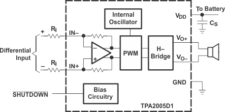
The TPA2005D1 is a 1.4-W high efficiency filter-free class-D audio power amplifier in a MicroStar Junior™ BGA, QFN, or MSOP package that requires only three external components.
Features like 84% efficiency, –71-dB PSRR
at 217 Hz, improved RF-rectification immunity, and
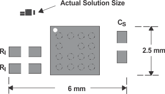
15 mm2 total PCB area make the TPA2005D1 ideal for cellular handsets. A fast start-up time of 9 ms with minimal pop makes the TPA2005D1 ideal for PDA applications.
In cellular handsets, the earpiece, speaker phone, and melody ringer can each be driven by the TPA2005D1. The device allows independent gain control by summing the signals from each function while minimizing noise to only 48 μVRMS.
The TPA2005D1 has short-circuit and thermal protection.
Device Information(1)
| PART NUMBER | PACKAGE | BODY SIZE (NOM) |
|---|---|---|
| TPA2005D1 | HVSSOP (8) | 3.00 mm × 3.00 mm |
| VSON (8) | 3.00 mm x 3.00 mm | |
| BGA MICROSTAR JUNIOR (15) | 2.50 mm x 2.50 mm |
- For all available packages, see the orderable addendum at the end of the datasheet.
Device Layout and Size

Application Circuit
