SNAS519H July 2011 – August 2015 ADC12D1000RF , ADC12D1600RF
PRODUCTION DATA.
- 1 Device Overview
- 2 Revision History
- 3 Pin Configuration and Functions
-
4 Specifications
- 4.1 Absolute Maximum Ratings
- 4.2 ESD Ratings
- 4.3 Recommended Operating Conditions
- 4.4 Thermal Information
- 4.5 Electrical Characteristics: Static Converter
- 4.6 Electrical Characteristics: Dynamic Converter
- 4.7 Electrical Characteristics: Analog Input/Output and Reference
- 4.8 Electrical Characteristics: I-Channel to Q-Channel
- 4.9 Electrical Characteristics: Sampling Clock
- 4.10 Electrical Characteristics: AutoSync Feature
- 4.11 Electrical Characteristics: Digital Control and Output Pin
- 4.12 Electrical Characteristics: Power Supply
- 4.13 Electrical Characteristics: AC
- 4.14 Timing Requirements: Serial Port Interface
- 4.15 Timing Requirements: Calibration
- 4.16 Typical Characteristics
-
5 Detailed Description
- 5.1 Overview
- 5.2 Functional Block Diagram
- 5.3 Feature Description
- 5.4 Device Functional Modes
- 5.5
Programming
- 5.5.1
Control Modes
- 5.5.1.1
Non-Extended Control Mode
- 5.5.1.1.1 Dual Edge Sampling Pin (DES)
- 5.5.1.1.2 Non-Demultiplexed Mode Pin (NDM)
- 5.5.1.1.3 Dual Data Rate Phase Pin (DDRPh)
- 5.5.1.1.4 Calibration Pin (CAL)
- 5.5.1.1.5 Calibration Delay Pin (CalDly)
- 5.5.1.1.6 Power-Down I-channel Pin (PDI)
- 5.5.1.1.7 Power-Down Q-channel Pin (PDQ)
- 5.5.1.1.8 Test Pattern Mode Pin (TPM)
- 5.5.1.1.9 Full-Scale Input Range Pin (FSR)
- 5.5.1.1.10 AC- and DC-Coupled Mode Pin (VCMO)
- 5.5.1.1.11 LVDS Output Common-mode Pin (VBG)
- 5.5.1.2 Extended Control Mode
- 5.5.1.1
Non-Extended Control Mode
- 5.5.1
Control Modes
- 5.6 Register Maps
- 6 Application and Implementation
- 7 Power Supply Recommendations
- 8 Layout
- 9 Device and Documentation Support
- 10Mechanical, Packaging, and Orderable Information
1 Device Overview
1.1 Features
- Excellent Noise and Linearity up to and Above fIN = 2.7 GHz
- Configurable to Either 3.2 or 2 GSPS Interleaved or 1600 or 1000 MSPS Dual ADC
- New DESCLKIQ Mode for High Bandwidth, High Sampling Rate Apps
- Pin-Compatible With ADC10D1x00, ADC12D1x00
- AutoSync Feature for Multi-Chip Synchronization
- Internally Terminated, Buffered, Differential Analog Inputs
- Interleaved Timing Automatic and Manual Skew Adjust
- Test Patterns at Output for System Debug
- Time Stamp Feature to Capture External Trigger
- Programmable Gain, Offset, and tAD Adjust Feature
- 1:1 Non-Demuxed or 1:2 Demuxed LVDS Outputs
- Key Specifications
- Resolution 12 Bits
- Interleaved 3.2- and 2-GSPS ADC
- IMD3 (Fin = 2.7 GHz at –13 dBFS) –63.7/–73 dBFS (Typical)
- IMD3 (Fin = 2.7 GHz at –16 dBFS) –66.7/–85 dBFS (Typical)
- Noise Floor –154.6/–154 dBm/Hz (Typical)
- Power 3.94/3.42 W (Typical)
- Dual 1600/1000 MSPS ADC, Fin = 498 MHz
- ENOB 9.2/9.4 Bits (Typical)
- SNR 58.2/58.8 dB (Typical)
- SFDR 66.7/71.9 dBc (Typical)
- Power per Channel 1.97/1.71 W (Typical)
1.2 Applications
- 3G/4G Wireless Basestations
- Receive Path
- DPD Path
- Wideband Microwave Backhaul
- RF Sampling Software Defined Radios
- Military Communications
- SIGINT
- RADAR and LIDAR
- Wideband Communications
- Consumer RFs
- Tests and Measurements
1.3 Description
The 12-bit 3.2- and 2-GSPS ADC12D1x00RF is an RF-sampling GSPS ADC that can directly sample input frequencies up to and above 2.7 GHz. The ADC12D1x00RF augments the very large Nyquist zone of TI’s GSPS ADCs with excellent noise and linearity performance at RF frequencies, extending its usable range beyond the 3rd Nyquist zone
The ADC12D1x00RF provides a flexible LVDS interface which has multiple SPI programmable options to facilitate board design and FPGA/ASIC data capture. The LVDS outputs are compatible with IEEE 1596.3-1996 and supports programmable common-mode voltage. The product is packaged in a lead-free 292-ball thermally enhanced BGA package over the rated industrial temperature range of –40°C to 85°C.
Device Information(1)
| PART NUMBER | PACKAGE | BODY SIZE |
|---|---|---|
| ADC12D1000RF | BGA (40) | 27.00 mm × 27.00 mm |
| ADC12D1600RF |
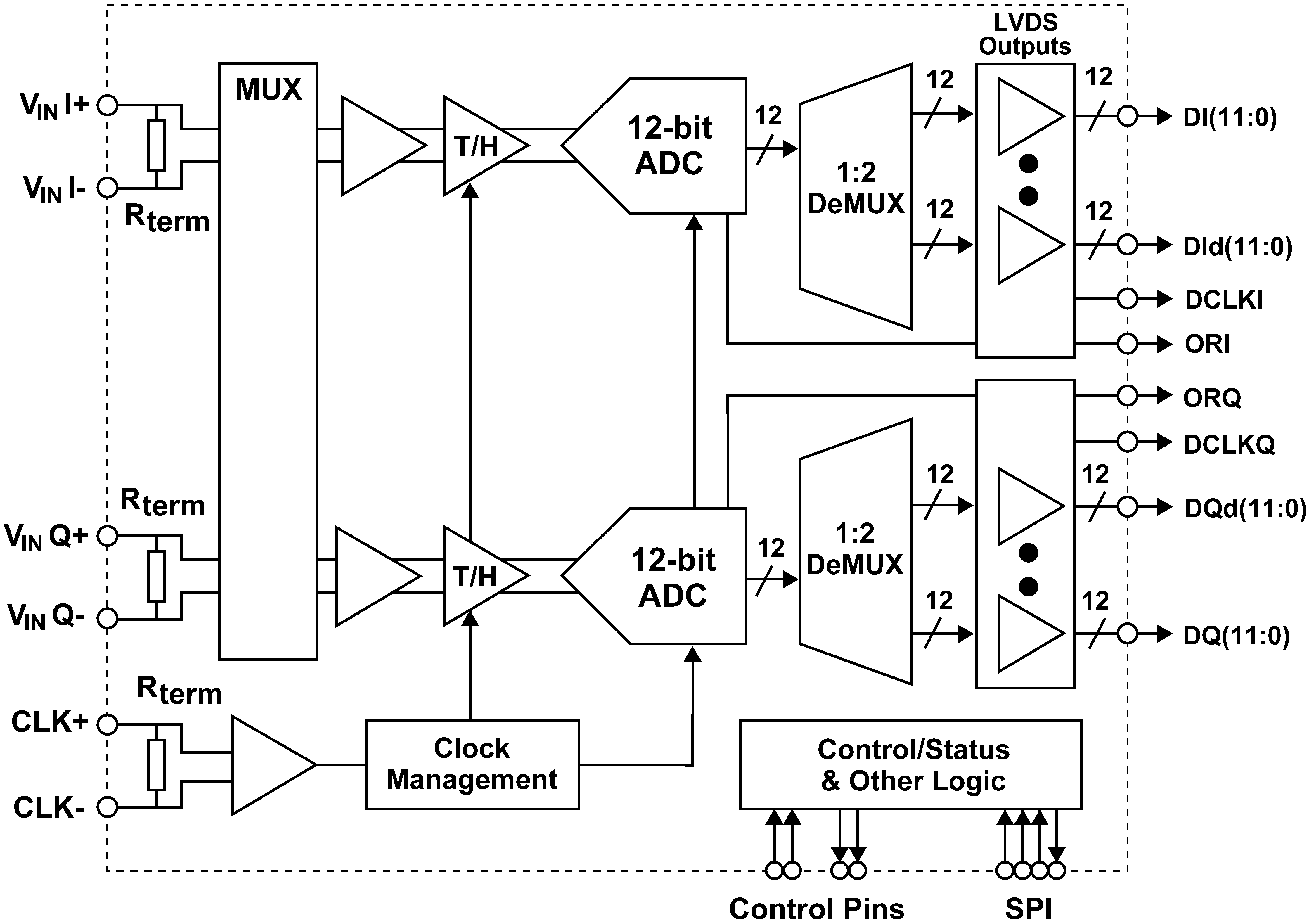
1.4 Functional Block Diagram
