SLAS525D July 2007 – December 2017 ADS5474
PRODUCTION DATA.
1 Features
- 400-MSPS Sample Rate
- 14-Bit Resolution, 11.2-Bits ENOB
- 1.4-GHz Input Bandwidth
- 80-dBc SFDR at 230 MHz and 400 MSPS
- 69.8-dBFS SNR at 230 MHz and 400 MSPS
- 2.2-VPP Differential Input Voltage
- LVDS-Compatible Outputs
- 2.5-W Total Power Dissipation
- 50-mW Power-Down Mode
- Offset Binary Output Format
- Output Data Transitions on the Rising and Falling Edges of a Half-Rate Output Clock
- On-Chip Analog Buffer, Track-and-Hold, and Reference Circuit
- HTQFP-80 PowerPAD™ Package
(14-mm × 14-mm Footprint) - Industrial Temperature Range:
–40°C to +85°C - Pin-Similar, -Compatible With 12-, 13-, and 14-Bit Family: ADS5463, ADS5440, ADS5444
2 Applications
- Test and Measurement Instrumentation
- Software-Defined Radio
- Data Acquisition
- Power Amplifier Linearization
- Communication Instrumentation
- Radar
3 Description
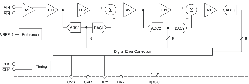
The ADS5474 device is a 14-bit, 400-MSPS analog-to-digital converter (ADC) that operates from both a 5-V supply and 3.3-V supply while providing LVDS-compatible digital outputs. This ADC is one of a family of 12-, 13-, and 14-bit ADCs that operate from 210 MSPS to 500 MSPS. The ADS5474 device has an input buffer that isolates the internal switching of the onboard track and hold (T&H) from disturbing the signal source while providing a high-impedance input. An internal reference generator is also provided to simplify the system design.
Designed with a 1.4-GHz input bandwidth for the conversion of wide-bandwidth signals that exceed 400 MHz of input frequency at 400 MSPS, the ADS5474 device has outstanding low-noise performance and spurious-free dynamic range over a large input frequency range.
The ADS5474 device is available in an TQFP-80 PowerPAD package. The device is built on Texas Instruments complementary bipolar process (BiCom3) and is specified over the full industrial temperature range (–40°C to +85°C).
Device Information(1)
| PART NUMBER | PACKAGE | BODY SIZE (NOM) |
|---|---|---|
| ADS5474 | HTQFP (80) | 12.00 mm x 12.00 mm |
- For all available packages, see the orderable addendum at the end of the data sheet.
Block Diagram
