SLAS638A January 2009 – October 2015 SN65HVS885
PRODUCTION DATA.
- 1 Features
- 2 Applications
- 3 Description
- 4 Revision History
- 5 Pin Configuration and Functions
- 6 Specifications
- 7 Parameter Measurement Information
- 8 Detailed Description
- 9 Application and Implementation
- 10Power Supply Recommendations
- 11Layout
- 12Device and Documentation Support
- 13Mechanical, Packaging, and Orderable Information
1 Features
- Eight Digital Sensor Inputs
- Single 5-V Supply
- Output Drivers for External Status LEDs
- Cascadable for More Inputs in Multiples of Eight
- SPI-Compatible Interface
- Overtemperature Indicator
2 Applications
- Industrial PCs
- Digital I/O Cards
- High Channel Count Digital Input Modules
- Decentralized I/O Modules
3 Description
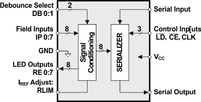
The SN65HVS885 is an eight channel, digital-input serializer for high-channel density digital input modules in industrial and building automation. Operating from a 5-V supply the device accepts field input voltages of up to 34 V. In combination with galvanic isolators the device completes the interface between the high voltage signals on the field-side and the low-voltage signals on the controller side. Inputs signals are current limited and then validated by internal debounce filters.
With the addition of few external components, the input switching characteristic can be configured in accordance with IEC61131-2 for Type 1, 2 and 3 sensor switches.
Upon the application of load and clock signals, input data is latched in parallel into the shift register and afterwards clocked out serially.
Cascading of multiple devices is possible by connecting the serial output of the leading device with the serial input of the following device, enabling the design of high-channel count input modules. Multiple devices can be cascaded through a single serial port, reducing both the isolation channels and controller inputs required.
Input status can be visually indicated via constant current LED outputs. The current limit on the inputs is set by a single, external, precision resistor. An on-chip temperature sensor provides diagnostic information for graceful shutdown and system safety.
The SN65HVS885 is available in a 28-pin PWP PowerPAD™ package, allowing for efficient heat dissipation. The device is specified for operation at temperatures from –40°C to 125°C.
Device Information(1)
| PART NUMBER | PACKAGE | BODY SIZE (NOM) |
|---|---|---|
| SN65HVS885 | HTSSOP (28) | 9.70 mm × 4.40 mm |
- For all available packages, see the orderable addendum at the end of the datasheet.
Simplified I/O Structure

4 Revision History
Changes from * Revision (January 2009) to A Revision
- Added Pin Configuration and Functions section, ESD Ratings table, Feature Description section, Device Functional Modes, Application and Implementation section, Power Supply Recommendations section, Layout section, Device and Documentation Support section, and Mechanical, Packaging, and Orderable Information section Go