SLVSCA0C October 2013 – September 2016
PRODUCTION DATA.
- 1 Features
- 2 Applications
- 3 Description
- 4 Revision History
- 5 Pin Configuration and Functions
- 6 Specifications
- 7 Detailed Description
- 8 Application and Implementation
- 9 Power Supply Recommendations
- 10Layout
- 11Device and Documentation Support
- 12Mechanical, Packaging, and Orderable Information
1 Features
- Qualified for Automotive Applications
- AEC-Q100 Qualified With the Following Results
- –20-V to 45-V Wide, Maximum Input Voltage Range
- Output Current, 50 mA
- Very-Low Output-Tracking Tolerance,
5 mV (max) - 150-mV Low Dropout Voltage When
IOUT = 10 mA - Combined Reference and Enable Input
- 40-µA Low Quiescent Current at Light Load
- Extreme, Wide ESR Range.
- Stable with 1-µF to 50-µF Ceramic Output Capacitor, ESR 1 mΩ to 20 Ω
- Reverse Polarity Protection
- Overtemperature Protection
- Output Short-Circuit Proof to Ground and Supply
- SOT-23 Package
2 Applications
- Off-board Sensor Supply
- High-Precision Voltage Tracking
3 Description
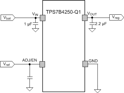
The TPS7B4250-Q1 device is a monolithic, integrated low-dropout voltage tracker. The device is available in a SOT-23 package. The TPS7B4250-Q1 device is designed to supply off-board sensors in an automotive environment. The IC has integrated protection for overload, over temperature, reverse polarity, and output short-circuit to the battery and ground.
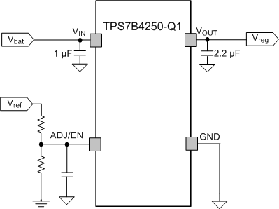
A reference voltage applied at the adjust-input pin, ADJ, regulates supply voltages up to VIN = 45 V with high accuracy and loads up to 50 mA.
By setting the adjust/enable input pin, ADJ/EN, to low, the TPS7B4250-Q1 device switches to standby mode which reduces the quiescent current to the minimum value.
Device Information(1)
| PART NUMBER | PACKAGE | BODY SIZE (NOM) |
|---|---|---|
| TPS7B4250-Q1 | SOT-23 (5) | 2.90 mm × 1.60 mm |
- For all available packages, see the orderable addendum at the end of the data sheet.

