SNVS820B APRIL 2013 – December 2016
PRODUCTION DATA.
- 1 Features
- 2 Applications
- 3 Description
- 4 Revision History
- 5 Pin Configuration and Functions
-
6 Specifications
- 6.1 Absolute Maximum Ratings
- 6.2 ESD Ratings
- 6.3 Recommended Operating Conditions
- 6.4 Thermal Information
- 6.5 Electrical Characteristics
- 6.6 Logic Interface Characteristics
- 6.7 Recommended External Clock Source Conditions
- 6.8 I2C Timing Requirements (SDA, SCL)
- 6.9 Typical Characteristics: Current Consumption
- 6.10 Typical Characteristics: LED Output
-
7 Detailed Description
- 7.1 Overview
- 7.2 Functional Block Diagram
- 7.3
Feature Description
- 7.3.1 LED Drivers Operational Description
- 7.3.2 Direct I2C Register PWM Control Example
- 7.3.3 Program Execution Engines
- 7.3.4 Power-Save Mode
- 7.3.5 External Clock
- 7.3.6 Thermal Shutdown
- 7.3.7 Logic Interface Operational Description
- 7.3.8 I/O Levels
- 7.3.9 ADDR_SEL0, ADDR_SEL1 Pins
- 7.3.10 CLK_32 Pin
- 7.4 Device Functional Modes
- 7.5 Programming
- 7.6
Register Maps
- 7.6.1 Enable Register (Enable) (Address = 00h) [reset = 00h]
- 7.6.2 Operation Mode Register (OP Mode) (address = 01h) [reset = 00h]
- 7.6.3 B LED Output PWM Control Register (B_PWM) (address = 02h) [reset = 00h]
- 7.6.4 G LED Output PWM Control Register (G_PWM) (address = 03h) [reset = 00h]
- 7.6.5 R LED Output PWM Control Register (R_PWM) (address = 04h) [reset = 00h]
- 7.6.6 B LED Output Current Control Register (B_CURRENT)(address = 05h) [reset = AFh]
- 7.6.7 G LED Output Current Control Register (G_CURRENT)(address = 06h) [reset = AFh]
- 7.6.8 R LED Output Current Control Register (R_CURRENT) (address = 07h) [reset = AFh]
- 7.6.9 Configuration Control Register (CONFIG) (address = 08h) [reset = 00h]
- 7.6.10 Engine 1 Program Counter Value Register (Engine 1 PC) (address = 09h) [reset = 00h]
- 7.6.11 Engine 2 Program Counter Value Register (Engine 2 PC) (address = 0Ah) [reset = 00h]
- 7.6.12 Engine 3 Program Counter Value Register (Engine 3 PC) (address = 0Ah) [reset = 00h]
- 7.6.13 STATUS/INTERRUPT Register (address = 0Ch) [reset = 00h]
- 7.6.14 RESET Register (address = 0Dh) [reset = 00h]
- 7.6.15 WLED Output PWM Control Register (W_PWM) (address = 0Eh) [reset = 00h]
- 7.6.16 W LED Output Current Control Register (W_CURRENT) (address = 0Fh) [reset = AFh]
- 7.6.17 LED Mapping Register (LED Map) (address = 70h) [reset = 39h]
- 7.6.18 Program Memory (address = 10h - 6Fh) [reset = 00h]
- 8 Application and Implementation
- 9 Power Supply Recommendation
- 10Layout
- 11Device and Documentation Support
- 12Mechanical, Packaging, and Orderable Information
1 Features
- Four Independently Programmable LED Outputs With 8-Bit Current Setting (From 0 mA to 25.5 mA With 100-μA Steps) and 8-Bit PWM Control
- Typical LED Output Saturation Voltage 60 mV and Current Matching 1%
- Flexible PWM Control for LED Outputs
- Automatic Power-Save Mode With External Clock
- Three Program Execution Engines With Flexible Instruction Set
- Autonomous Operation With Program Execution Engines
- SRAM Program Memory for Lighting Pattern Programs
- DSBGA 12-Pin Package, 0.4-mm Pitch
2 Applications
- Fun Lights
- Indicator Lights
- Keypad RGB Backlighting and Phone Cosmetics
3 Description
The LP5562 is a four-channel LED driver designed to produce variety of lighting effects. The device has a program memory for creating variety of lighting sequences. When the program memory has been loaded, the LP5562 can operate independently without processor control.
The LP5562 is able to automatically enter power save mode, when LED outputs are not active and thus lowering current consumption.
Four independent LED channels have accurate programmable current sinks, from 0 mA to 25.5 mA with 100-μA steps and flexible PWM control. Each channel can be configured into each of the three program execution engines. Program execution engines have program memory for creating desired lighting sequences with PWM control.
The LP5562 has four pin-selectable I2C addresses. This allows connecting up to four parallel devices in one I2C bus. The device requires only one small, low-cost ceramic capacitor.
Device Information(1)
| PART NUMBER | PACKAGE | BODY SIZE (MAX) |
|---|---|---|
| LP5562 | DSBGA (12) | 1.648 mm × 1.248 mm |
- For all available packages, see the orderable addendum at the end of the data sheet.
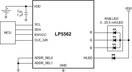
Typical Application Diagram
