SNVS576F August 2008 – February 2015 LM26003 , LM26003-Q1
PRODUCTION DATA.
- 1 Features
- 2 Applications
- 3 Description
- 4 Typical Application Circuit
- 5 Revision History
- 6 Pin Configuration and Functions
- 7 Specifications
- 8 Detailed Description
- 9 Application and Implementation
- 10Power Supply Recommendations
- 11Layout
- 12Device and Documentation Support
- 13Mechanical, Packaging, and Orderable Information
1 Features
- LM26003-Q1 is an Automotive-Grade Product That is AEC-Q100 Grade 1 Qualified (–40°C to +125°C Operating Junction Temperature)
- High-Efficiency Sleep Mode
- 40-µA Typical Iq in Sleep Mode
- 10.8-µA Typical Iq in Shutdown Mode
- 3.0-V Minimum Input Voltage
- 4.0-V to 38-V Continuous Input Range
- 1.5% Reference Accuracy
- Cycle-by-Cycle Current Limit
- Adjustable Frequency (150 kHz to 500 kHz)
- Synchronizable to an External Clock
- Power Good Flag
- Forced PWM Function
- Adjustable Soft-Start
- 20-Pin HTSSOP Package
- Thermal Shut Down
2 Applications
- Automotive Telematics
- Navigation Systems
- In-Dash Instrumentation
- Battery-Powered Applications
- Standby Power for Home Gateways and Set-Top Boxes
3 Description
The LM26003 is a switching regulator designed for the high-efficiency requirements of applications with standby modes. The device features a low-current sleep mode to maintain efficiency under light-load conditions and current-mode control for accurate regulation over a wide input voltage range. Quiescent current is reduced to 10.8 µA typically in shutdown mode and less than 40 µA in sleep mode. Forced PWM mode is also available to disable sleep mode.
The LM26003 device can deliver up to 3 A of continuous load current with a fixed current limit, through the internal N-channel switch. The part has a wide input voltage range of 4.0 V to 38 V and can operate with input voltages as low as 3 V during line transients.
Operating frequency is adjustable from 150 kHz to 500 kHz with a single resistor and can be synchronized to an external clock.
Other features include Power Good, adjustable soft-start, enable pin, input undervoltage protection, and an internal bootstrap diode for reduced component count.
Device Information(1)
| PART NUMBER | PACKAGE | BODY SIZE (NOM) |
|---|---|---|
| LM26003 | HTSSOP (20) | 6.50 mm x 4.40 mm |
| LM26003-Q1 |
- For all available packages, see the orderable addendum at the end of the datasheet.
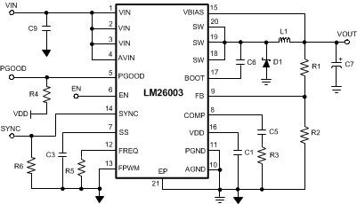
4 Typical Application Circuit
