SNOS519K April 2000 – August 2016 LMV710-N
PRODUCTION DATA.
- 1 Features
- 2 Applications
- 3 Description
- 4 Revision History
- 5 Pin Configuration and Functions
- 6 Specifications
- 7 Detailed Description
- 8 Application and Implementation
- 9 Power Supply Recommendations
- 10Layout
- 11Device and Documentation Support
- 12Mechanical, Packaging, and Orderable Information
1 Features
- Low Offset Voltage: 3 mV (Maximum)
- Gain-Bandwidth Product: 5 MHz (Typical)
- Slew Rate: 5 V/µs (Typical)
- Space-Saving Packages: 5-Pin and 6-Pin SOT-23
- Turnon Time From Shutdown: <10 µs
- Industrial Temperature Range: −40°C to 85°C
- Supply Current in Shutdown Mode: 0.2 µA (Typical)
- Ensured 2.7-V and 5-V Performance
- Unity Gain Stable
- Rail-to-Rail Input and Output
- Capable of Driving 600-Ω Load
2 Applications
- Wireless Phones
- GSM, TDMA, and CDMA Power Amp Controls
- AGC and RF Power Detectors
- Temperature Compensation
- Wireless LAN
- Bluetooth
- HomeRF
3 Description
The LMV710-N, LMV711-N, and LMV715-N are BiCMOS operational amplifiers with a CMOS input stage. These devices have greater than RR input common mode voltage range, rail-to-rail output and high output current drive. They offer a bandwidth of
5 MHz and a slew rate of 5 V/µs.
On the LMV711 and LMV715, a separate shutdown pin can be used to disable the device and reduces the supply current to 0.2 µA (typical). They also feature a turnon time of less than 10 µs. It is an ideal solution for power-sensitive applications, such as cellular phone, pager, palm computer, and so forth. In addition, once the LMV715 is in shutdown the output is tri-stated.
The LMV710 is offered in the space-saving, 5-pin SOT-23 package. The LMV711 and LMV715 are offered in the space saving 6-pin SOT-23 package.
The LMV71x-N devices are designed to meet the demands of low power, low cost, and small size required by cellular phones and similar battery-powered portable electronics.
Device Information(1)
| PART NUMBER | PACKAGE | BODY SIZE (NOM) |
|---|---|---|
| LMV710-N | SOT-23 (5) | 2.92 mm × 1.50 mm |
| LMV711-N LMV715-N |
SOT-23 (6) | 2.92 mm × 1.50 mm |
- For all available packages, see the orderable addendum at the end of the data sheet.
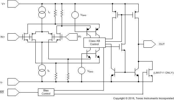
Simplified Schematic – LMV711
