SLVS928B March 2009 – August 2014 TPD4S012
UNLESS OTHERWISE NOTED, this document contains PRODUCTION DATA.
1 Features
2 Applications
- Cellular Phones
- Digital Cameras
- Global Positioning Systems (GPS)
- Portable Digital Assistants (PDA)
- Portable Computers
3 Description
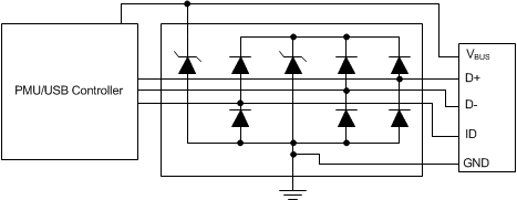
The TPD4S012 is a four-channel Transient Voltage Suppressor (TVS) based Electrostatic Discharge (ESD) protection diode array for USB chargers and USB On-The-Go (OTG) interfaces.
The TPD4S012 provides IEC 61000-4-2 system level ESD Protection featuring 15 V tolerance on the VBUS line. The device is ideal for providing circuit protection for USB charger and OTG applications due to its high-voltage tolerance at the VBUS line and small flow-through package.
Device Information(1)
| PART NUMBER | PACKAGE | BODY SIZE (NOM) |
|---|---|---|
| TPD4S012 | SON (6) | 1.45 mm x 1.00 mm |
- For all available packages, see the orderable addendum at the end of the datasheet.
Typical Application Schematic