SLVSAD5A July 2010 – August 2015 TPS62120 , TPS62122
PRODUCTION DATA.
- 1 Features
- 2 Applications
- 3 Description
- 4 Revision History
- 5 Device Comparison Table
- 6 Pin Configuration and Functions
- 7 Specifications
- 8 Detailed Description
- 9 Application and Implementation
- 10Power Supply Recommendations
- 11Layout
- 12Device and Documentation Support
- 13Mechanical, Packaging, and Orderable Information
1 Features
- Wide Input Voltage Range: 2 V to 15 V
- Up to 96% Efficiency
- Power Save Mode With 11-µA Quiescent Current
- Output Current 75 mA
- Output Voltage Range: 1.2 V to 5.5 V
- Up to 800-kHz Switch Frequency
- Synchronous Converter, No External Rectifier
- Low Output Ripple Voltage
- 100% Duty Cycle for Lowest Dropout
- Small SOT 8-Pin (TPS62120) and 2-mm × 2-mm DFN 6-Pin (TPS62122) Package
- Internal Soft Start
- Power Good Open Drain Output (TPS62120)
- Open-Drain Output for Output Discharge (TPS62120)
- 2.5-V Rising and 1.85-V Falling UVLO Thresholds
2 Applications
- Low Power RF Applications
- Ultra Low Power Microprocessors
- Energy Harvesting
- Industrial Measuring
3 Description
The TPS6212x device is a highly efficient synchronous step-down DC-DC converter optimized for low-power applications. The device supports up to 75-mA output current and allows the use of tiny external inductors and capacitors.
The wide operating input voltage range of 2 V to 15 V supports energy harvesting, battery powered and as well 9-V or 12-V line powered applications.
With its advanced hysteretic control scheme, the converter provides power save mode operation. At light loads the converter operates in pulse frequency modulation (PFM) mode and transitions automatically in pulse width modulation (PWM) mode at higher load currents. The power save mode maintains high efficiency over the entire load current range. The hysteretic control scheme is optimized for low output ripple voltage in PFM mode in order to reduce output noise to a minimum. The device consumes only 10-µA quiescent current from VIN in PFM mode operation.
In shutdown mode, the device is turned off.
An open-drain power good output is available in the TPS62120 and indicates once the output voltage is in regulation.
The TPS62120 has an additional SGND pin which is connected to GND during shutdown mode. This output can be used to discharge the output capacitor.
The TPS6212x operates over an free air temperature range of –40°C to 85°C. The TPS62120 is available in a small 8-pin SOT-23 package and the TPS62122 in a 2 mm × 2 mm 6-pin DFN package.
Device Information(1)
| PART NUMBER | PACKAGE | BODY SIZE (NOM) |
|---|---|---|
| TPS62120 | SOT-23 (8) | 2.90 mm × 1.63 mm |
| TPS62122 | SON (6) | 2.00 mm × 2.00 mm |
- For all available packages, see the orderable addendum at the end of the data sheet.
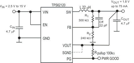
Typical Application Schematic

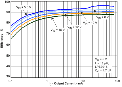
Efficiency vs Output Current
