SLVS497F SEPTEMBER 2003 – June 2016 TPS65140 , TPS65141 , TPS65145
PRODUCTION DATA.
- 1 Features
- 2 Applications
- 3 Description
- 4 Revision History
- 5 Pin Configuration and Functions
- 6 Specifications
- 7 Detailed Description
-
8 Application and Implementation
- 8.1 Application Information
- 8.2
Typical Application
- 8.2.1 Design Requirements
- 8.2.2
Detailed Design Procedure
- 8.2.2.1
Boost Converter Design Procedure
- 8.2.2.1.1 Inductor Selection
- 8.2.2.1.2 Output Capacitor Selection
- 8.2.2.1.3 Input Capacitor Selection
- 8.2.2.1.4 Rectifier Diode Selection
- 8.2.2.1.5 Converter Loop Design and Stability
- 8.2.2.1.6 Design Procedure Quick Steps
- 8.2.2.1.7 Setting the Output Voltage and Selecting the Feedforward Capacitor
- 8.2.2.1.8 Compensation
- 8.2.2.1.9 Negative Charge Pump
- 8.2.2.1.10 Positive Charge Pump
- 8.2.2.1.11 Linear Regulator Controller
- 8.2.2.1
Boost Converter Design Procedure
- 8.2.3 Application Curves
- 8.3 System Examples
- 9 Power Supply Recommendations
- 10Layout
- 11Device and Documentation Support
- 12Mechanical, Packaging, and Orderable Information
封装选项
请参考 PDF 数据表获取器件具体的封装图。
机械数据 (封装 | 引脚)
- RGE|24
- PWP|24
散热焊盘机械数据 (封装 | 引脚)
订购信息
1 Features
- 2.7-V to 5.8-V Input Voltage Range
- 1.6-MHz Fixed Switching Frequency
- 3 Independent Adjustable Outputs
- Main Output up to 15 V With <1% Typical Output Voltage Accuracy
- Virtual Synchronous Converter Technology
- Negative Regulated Charge Pump Driver VO2
- Positive Charge Pump Converter VO3
- Auxiliary 3.3-V Linear Regulator Controller
- Internal Soft Start
- Internal Power-On Sequencing
- Fault Detection of All Outputs (TPS65140 and TPS65145)
- No Fault Detection (TPS65141)
- Thermal Shutdown
- System Power Good
- Available in 24-Pin HTSSOP and 24-Pin VQFN PowerPAD™ Packages
2 Applications
- TFT LCD Displays for Notebooks
- TFT LCD Displays for Monitors
- Portable DVD Players
- Tablet PCs
- Car Navigation Systems
- Industrial Displays
3 Description
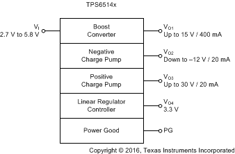
The TPS6514x series offers a compact and small power supply solution to provide all three voltages required by thin film transistor (TFT) LCD displays. The auxiliary linear regulator controller can be used to generate a 3.3-V logic power rail for systems powered by a 5-V supply rail only.
The main output VO1 is a 1.6-MHz fixed frequency PWM boost converter providing the source drive voltage for the LCD display. The device is available in two versions with different internal switch current limits to allow the use of a smaller external inductor when lower output power is required. The TPS65140 and TPS65141 has a typical switch current limit of 2.3 A and the TPS65145 has a typical switch current limit of 1.37 A. A fully integrated adjustable charge pump doubler or tripler provides the positive LCD gate drive voltage. An externally adjustable negative charge pump provides the negative gate drive voltage. Due to the high 1.6-MHz switching frequency of the charge pumps, inexpensive and small 220-nF capacitors can be used.
Additionally, the TPS6514x series has a system power good output to indicate when all supply rails are acceptable. For LCD panels powered by 5 V the device has a linear regulator controller using an external transistor to provide a regulated 3.3-V output for the digital circuits. For maximum safety, the TPS65140 and TPS65145 goes into shutdown as soon as one of the outputs is out of regulation. The device can be enabled again by toggling the input or the enable (EN) pin to GND. The TPS65141 does not enter shutdown when one of its outputs is below its power good threshold.
Device Information(1)
| PART NUMBER | PACKAGE | BODY SIZE (NOM) |
|---|---|---|
| TPS6514x | HTSSOP (24) | 7.80 mm × 4.40 mm |
| VQFN (24) | 4.00 mm × 4.00 mm |
- For all available packages, see the orderable addendum at the end of the data sheet.
4 Revision History
Changes from E Revision (November 2012) to F Revision
- Added ESD Ratings table, Thermal Information table, Feature Description section, Device Functional Modes section, Application and Implementation section, Power Supply Recommendations section, Layout section, Device and Documentation Support section, and Mechanical, Packaging, and Orderable Information sectionGo
- Deleted Ordering Information table; see POA at the end of the data sheetGo
- Changed typical value of VREF to 1.213 V from 1.13 VGo
- Moved Figure 12 through Figure 23 from Typical Applications to Application CurvesGo
