SLLSE39E June 2010 – May 2015 ISO7520C , ISO7521C
PRODUCTION DATA.
- 1 Features
- 2 Applications
- 3 Description
- 4 Revision History
- 5 Pin Configuration and Functions
-
6 Specifications
- 6.1 Absolute Maximum Ratings
- 6.2 ESD Ratings
- 6.3 Recommended Operating Conditions
- 6.4 Thermal Information
- 6.5 Electrical Characteristics: VCC1 and VCC2 at 5 V ± 5%
- 6.6 Electrical Characteristics: VCC1 at 5 V ± 5%, VCC2 at 3.3 V ± 5%
- 6.7 Electrical Characteristics: VCC1 at 3.3 V ± 5%, VCC2 at 5 V ± 5%
- 6.8 Electrical Characteristics: VCC1 and VCC2 at 3.3 V ± 5%
- 6.9 Switching Characteristics: VCC1 and VCC2 at 5 V ± 5%
- 6.10 Switching Characteristics: VCC1 at 5 V ± 5%, VCC2 at 3.3 V ± 5%
- 6.11 Switching Characteristics: VCC1 at 3.3 V ± 5%, VCC2 at 5 V ± 5%
- 6.12 Switching Characteristics: VCC1 and VCC2 at 3.3 V ± 5%
- 6.13 Typical Characteristics
- 7 Parameter Measurement Information
- 8 Detailed Description
- 9 Application and Implementation
- 10Power Supply Recommendations
- 11Layout
- 12Device and Documentation Support
- 13Mechanical, Packaging, and Orderable Information
Package Options
Mechanical Data (Package|Pins)
- DW|16
Thermal pad, mechanical data (Package|Pins)
- DW|16
Orderable Information
1 Features
- Highest Signaling Rate: 1 Mbps
- Propagation Delay Less Than 20 ns
- Low-Power Consumption
- Wide Ambient Temperature: –40°C to 105°C
- 50 kV/µs Transient Immunity Typical
- Operates From 3.3-V or 5-V Supply and Logic Levels
- 3.3-V and 5.0-V Level Translation
- Safety and Regulatory Approvals
- 6000 VPK Isolation per DIN V VDE V 0884-10 and DIN EN 61010-1
- 4243 VRMS Isolation for 1 Minute per UL 1577
- CSA Component Acceptance Notice 5A, IEC 60950-1, IEC 61010-1, and IEC 60601-1 End Equipment Standards
- TUV 5000 VRMS Isolation per EN 60950-1 and EN 61010-1
- CQC Certification per GB4943.1-2011
2 Applications
- Opto-Coupler Replacement in:
- Industrial Field-Buses
- ProfiBuses
- ModBuses
- DeviceNet™ Data Buses
- Servo Control Interfaces
- Motor Control
- Power Supplies
- Battery Packs
- Industrial Field-Buses
3 Description
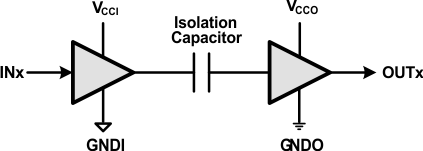
The ISO7520C and ISO7521C provide galvanic isolation of up to 4243 VRMS for 1 minute per UL and 6000 VPK per VDE. These devices are also certified to 5000 VRMS reinforced insulation per end equipment standards IEC 60950-1, IEC 61010-1, and IEC 60601-1. These digital isolators have two isolated channels with unidirectional (ISO7520C) and bidirectional (ISO7521C) channel configurations. Each isolation channel has a logic input and output buffer separated by a silicon oxide (SiO2) insulation barrier. Used in conjunction with isolated power supplies, these devices prevent noise currents on a data bus or other circuits from entering the local ground and interfering with or damaging sensitive circuitry. The devices have TTL input thresholds and can operate from 3.3- and 5-V supplies. All inputs are 5-V tolerant when supplied from 3.3-V supplies.
NOTE: The ISO7520C and ISO7521C are specified for signaling rates up to 1 Mbps. Due to their fast response time, these devices will also transmit faster data with much shorter pulse widths. Designers must add external filtering to remove spurious signals with input pulse duration < 20 ns, if desired.
Device Information(1)
| PART NUMBER | PACKAGE | BODY SIZE (NOM) |
|---|---|---|
| ISO7520C | SOIC (16) | 10.30 mm × 7.50 mm |
| ISO7521C |
- For all available packages, see the orderable addendum at the end of the data sheet.
Simplified Schematic
