SCLS336I January 2000 – August 2014 SN74AHCT16373
UNLESS OTHERWISE NOTED, this document contains PRODUCTION DATA.
- 1 Features
- 2 Applications
- 3 Description
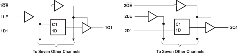
- 4 Simplified Schematic
- 5 Revision History
- 6 Pin Configuration and Functions
- 7 Specifications
- 8 Parameter Measurement Information
- 9 Detailed Description
- 10Application and Implementation
- 11Power Supply Recommendations
- 12Layout
- 13Device and Documentation Support
- 14Mechanical, Packaging, and Orderable Information
パッケージ・オプション
デバイスごとのパッケージ図は、PDF版データシートをご参照ください。
メカニカル・データ(パッケージ|ピン)
- DGG|48
- DL|48
- DGV|48
サーマルパッド・メカニカル・データ
発注情報
1 Features
- Members of the Texas Instruments Widebus™ Family
- EPIC™ (Enhanced-Performance Implanted CMOS) Process
- Inputs are TTL-Voltage Compatible
- Distributed VCC and GND Pins Minimize High-Speed Switching Noise
- Flow-Through Architecture Optimizes PCB Layout
- Latch-Up Performance Exceeds 250 mA Per JESD 17
- ESD Protection Exceeds 2000 V Per MIL-STD-883, Method 3015; Exceeds 200 V Using Machine Model (C = 200 pF, R = 0)
- Package Options Include:
- Plastic Shrink Small-Outline (DL) Package
- Thin Shrink Small-Outline (DGG) Package
- Thin Very Small-Outline (DGV) Package
- 80-mil Fine-Pitch Ceramic Flat (WD) Package Using 25-mil Center-to-Center Spacings
2 Applications
- Wearable Health and Fitness Devices
- Toys
- PCs and Notebooks
- Power Infrastructures
- Servers
3 Description
The SNxAHCT16373 devices are 16-bit transparent D-type latches with 3-state outputs designed specifically for driving highly capacitive or relatively low-impedance loads. They are particularly suitable for implementing buffer registers, I/O ports, bidirectional bus drivers, and working registers.
Device Information(1)
| PART NUMBER | PACKAGE | BODY SIZE (NOM) |
|---|---|---|
| SNx4AHC16373 | TSSOP (48) | 12.50 mm × 6.10 mm |
| TVSOP (48) | 9.70 mm × 4.40 mm | |
| SSOP (48) | 15.88 mm × 7.49 mm |
- For all available packages, see the orderable addendum at the end of the data sheet.
4 Simplified Schematic