SCAS572L April 1996 – July 2014 SN74LVC2244A
PRODUCTION DATA.
- 1 Features
- 2 Applications
- 3 Description
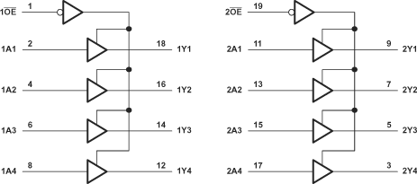
- 4 Simplified Schematic
- 5 Revision History
- 6 Pin Configuration and Functions
- 7 Specifications
- 8 Detailed Description
- 9 Application and Implementation
- 10Power Supply Recommendations
- 11Layout
- 12Device and Documentation Support
- 13Mechanical, Packaging, and Orderable Information
パッケージ・オプション
デバイスごとのパッケージ図は、PDF版データシートをご参照ください。
メカニカル・データ(パッケージ|ピン)
- DGV|20
- DB|20
- DBQ|20
- NS|20
- DW|20
- PW|20
サーマルパッド・メカニカル・データ
発注情報
1 Features
- Operates From 1.65 V to 3.6 V
- Inputs Accept Voltages to 5.5 V
- Max tpd of 5.5 ns at 3.3 V
- Output Ports Have Equivalent 26-Ω Series Resistors, So No External Resistors Are Required
- Typical VOLP (Output Ground Bounce)
<0.8 V at VCC = 3.3 V, TA = 25°C - Typical VOHV (Output VOH Undershoot)
>2 V at VCC = 3.3 V, TA = 25°C - Supports Mixed-Mode Signal Operation on All Ports (5-V Input/Output Voltage
With 3.3-V VCC) - Ioff Supports Live Insertion, Partial-Power-Down Mode, and Back-Drive Protection
- Latch-Up Performance Exceeds 250 mA Per JESD 17
- ESD Protection Exceeds JESD 22
- 2000-V Human-Body Model (A114-A)
- 200-V Machine Model (A115-A)
- 1000-V Charged-Device Model (C101)
3 Description
The SN74LVC2244A octal buffer/line driver is designed for 1.65-V to 3.6-V VCC operation.
Device Information(1)
| PART NUMBER | PACKAGE | BODY SIZE (NOM) |
|---|---|---|
| SN74LVC2244A | SSOP (20) | 7.20 mm × 5.30 mm |
| SSOP (20) | 8.65 mm × 3.90 mm | |
| TVSOP (20) | 5.00 mm × 4.40 mm | |
| SOIC (20) | 12.80 mm × 7.50 mm | |
| TSSOP (20) | 6.50 mm × 4.40 mm |
- For all available packages, see the orderable addendum at the end of the data sheet.
4 Simplified Schematic