-
ADS4229 Dual-Channel, 12-Bit, 250-MSPS Ultralow-Power ADC
- 1 Features
- 2 Applications
- 3 Description
- 4 Revision History
- 5 Device Comparison Table
- 6 Pin Configuration and Functions
-
7 Specifications
- 7.1 Absolute Maximum Ratings
- 7.2 ESD Ratings
- 7.3 Recommended Operating Conditions
- 7.4 Thermal Information
- 7.5 Electrical Characteristics: ADS4229 (250 MSPS)
- 7.6 Electrical Characteristics: General
- 7.7 Digital Characteristics
- 7.8 LVDS and CMOS Modes Timing Requirements
- 7.9 LVDS Timings at Lower Sampling Frequencies
- 7.10 CMOS Timings at Lower Sampling Frequencies
- 7.11 Serial Interface Timing Characteristics
- 7.12 Reset Timing (Only when Serial Interface is Used)
- 7.13 Typical Characteristics
-
8 Detailed Description
- 8.1 Overview
- 8.2 Functional Block Diagram
- 8.3 Feature Description
- 8.4 Device Functional Modes
- 8.5 Programming
- 8.6
Register Maps
- 8.6.1 Serial Register Map
- 8.6.2
Description of Serial Registers
- 8.6.2.1 Register Address 00h (Default = 00h)
- 8.6.2.2 Register Address 01h (Default = 00h)
- 8.6.2.3 Register Address 03h (Default = 00h)
- 8.6.2.4 Register Address 25h (Default = 00h)
- 8.6.2.5 Register Address 29h (Default = 00h)
- 8.6.2.6 Register Address 2Bh (Default = 00h)
- 8.6.2.7 Register Address 3Dh (Default = 00h)
- 8.6.2.8 Register Address 3Fh (Default = 00h)
- 8.6.2.9 Register Address 40h (Default = 00h)
- 8.6.2.10 Register Address 41h (Default = 00h)
- 8.6.2.11 Register Address 42h (Default = 00h)
- 8.6.2.12 Register Address 45h (Default = 00h)
- 8.6.2.13 Register Address 4Ah (Default = 00h)
- 8.6.2.14 Register Address 58h (Default = 00h)
- 8.6.2.15 Register Address BFh (Default = 00h)
- 8.6.2.16 Register Address C1h (Default = 00h)
- 8.6.2.17 Register Address CFh (Default = 00h)
- 8.6.2.18 Register Address EFh (Default = 00h)
- 8.6.2.19 Register Address F1h (Default = 00h)
- 8.6.2.20 Register Address F2h (Default = 00h)
- 8.6.2.21 Register Address 2h (Default = 00h)
- 8.6.2.22 Register Address D5h (Default = 00h)
- 8.6.2.23 Register Address D7h (Default = 00h)
- 8.6.2.24 Register Address DBh (Default = 00h)
- 9 Application and Implementation
- 10Power Supply Recommendations
- 11Layout
- 12Device and Documentation Support
- 13Mechanical, Packaging, and Orderable Information
- IMPORTANT NOTICE
ADS4229 Dual-Channel, 12-Bit, 250-MSPS Ultralow-Power ADC
1 Features
- Maximum Sample Rate: 250 MSPS
- Ultralow Power with Single 1.8-V Supply:
- 545-mW Total Power at 250 MSPS
- High Dynamic Performance:
- Crosstalk: > 90 dB at 185 MHz
- Programmable Gain Up to 6 dB for
SNR and SFDR Trade-off - DC Offset Correction
- Output Interface Options:
- 1.8-V Parallel CMOS Interface
- DDR LVDS With Programmable Swing:
- Standard Swing: 350 mV
- Low Swing: 200 mV
- Supports Low Input Clock Amplitude
Down to 200 mVPP - Package: 9-mm × 9-mm, 64-Pin Quad Flat
No-Lead (QFN) Package
2 Applications
- Wireless Communications Infrastructure
- Software Defined Radio
- Power Amplifier Linearization
3 Description
The ADS4229 is a member of the ADS42xx ultralow-power family of dual-channel, 12-bit and 14-bit analog-to-digital converters (ADCs). Innovative design techniques are used to achieve high dynamic performance, while consuming extremely low power with a 1.8-V supply. This topology makes the ADS4229 well-suited for multi-carrier, wide-bandwidth communications applications.
The ADS4229 has gain options that can be used to improve spurious-free dynamic range (SFDR) performance at lower full-scale input ranges. This device also includes a dc offset correction loop that can be used to cancel the ADC offset. Both double data rate (DDR) low-voltage differential signaling (LVDS) and parallel complementary metal oxide semiconductor (CMOS) digital output interfaces are available in a compact QFN-64 PowerPAD™ package.
The device includes internal references while the traditional reference pins and associated decoupling capacitors have been eliminated. The ADS4229 is specified over the industrial temperature range (–40°C to +85°C).
Device Information(1)
| PART NUMBER | PACKAGE | BODY SIZE (NOM) |
|---|---|---|
| ADS4229 | VQFN (64) | 9.00 mm × 9.00 mm |
- For all available packages, see the orderable addendum at the end of the datasheet.
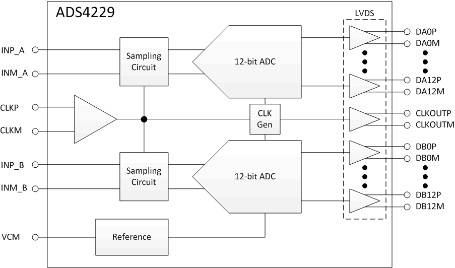
ADS4229 Block Diagram

4 Revision History
Changes from B Revision (August 2012) to C Revision
- Added Pin Configuration and Functions section, ESD Rating table, Feature Description section, Device Functional Modes, Application and Implementation section, Power Supply Recommendations section, Layout section, Device and Documentation Support section, and Mechanical, Packaging, and Orderable Information section Go
Changes from A Revision (October 2011) to B Revision
- Changed first sub-bullet of High Dynamic Performance Features bulletGo
- Changed footnote 1 in CMOS Timings at Lower Sampling FrequenciesGo
- Changed row D5 and consolidated the two DB rows in Table 10Go
- Changed Register Address D5hGo
- Changed title of Register Address DBh, consolidated two DBh registers into oneGo
Changes from * Revision (June 2011) to A Revision
- Changed ADS4229 Input Common-Mode Voltage parameter in Table 1Go
- Changed AC power-supply rejection ratio parameter test condition in ADS4229 Electrical Characteristics tableGo
- Updated Figure 3Go
- Updated Figure 25Go
- Updated Figure 31Go
- Updated Figure 32Go
- Changed Time Constant, TCCLK × 1/fS (ms) column and footnote 1 in Table 3Go
- Changed Revised Channel Standby sectionGo
- Changed High-performance mode parameter description in High-Performance Modes tableGo
- Changed description of bits[7:2] in Register Address 40hGo
- Updated Register Address D7h and Register Address D8h tablesGo
- Updated first paragraph of Analog Input sectionGo
- Updated first paragraph of Driving Circuit subsectionGo
5 Device Comparison Table
The ADS4229 is pin-compatible with the previous generation ADS62P49 data converter; this similar architecture enables easy migration. However, there are some important differences between the two device generations, summarized in Table 1.