SBOA292A April 2021 – February 2022 OPA192 , TLV9062
Design Goals
| Input | Output | BW | Supply | |||
|---|---|---|---|---|---|---|
| ViMin | ViMax | VoMin | VoMax | fp | Vcc | Vee |
| –2.5mV | 2.5mV | –2.5V | 2.5V | 5kHz | 5V | –5V |
Design Description
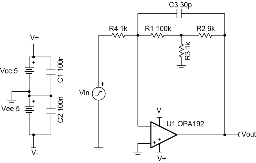
This design inverts the input signal, Vin, and applies a signal gain of 1000V/V or 60dB. The inverting amplifier with T-feedback network can be used to obtain a high gain without a small value for R4 or very large values for the feedback resistors.

Design Notes
- C3 and the equivalent resistance of feedback resistors set the cutoff frequency, fp.
- The common-mode voltage in this circuit does not vary with input voltage.
- Using high-value resistors can degrade the phase margin and increase noise.
- Avoid placing capacitive loads directly on the output of the amplifier to minimize stability issues.
- Due to the high gain of the circuit, be sure to use an op amp with sufficient gain bandwidth product. Remember to use the noise gain when calculating bandwidth. Use precision, or low offset, devices due to the high gain of the circuit.
- For more information on op amp linear operating region, stability, slew-induced distortion, capacitive load drive, driving ADCs, and bandwidth see the Design References section.
Design Steps
- Calculate required gain.
- Calculate resistor values to set the required gain.
Choose the input resistor R4 to be 1kΩ. To obtain a gain of 1000V/V, normally a 1-MΩ resistor would be required. A T-network allows us to use smaller resistor values in the feedback loop. Selecting R1 to be 100kΩ and R2 to be 9kΩ allows calculation of the value for R3. R2 is in the 10kΩ range so the op amp can easily drive the feedback network.
- Calculate C3 using the equivalent resistance of the feedback resistors, Req, to set the location of fp.
- Calculate the small signal circuit bandwidth to ensure it meets the 5 kHz requirement. Be sure to use the noise gain, NG, or non-inverting gain of the circuit.
- BWOPA192 = 10MHz; therefore this requirement is met.
Design Simulations
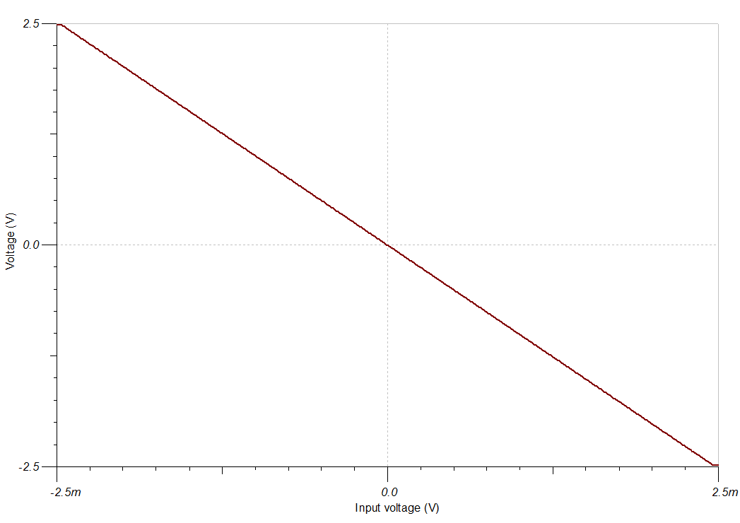
DC Simulation Results

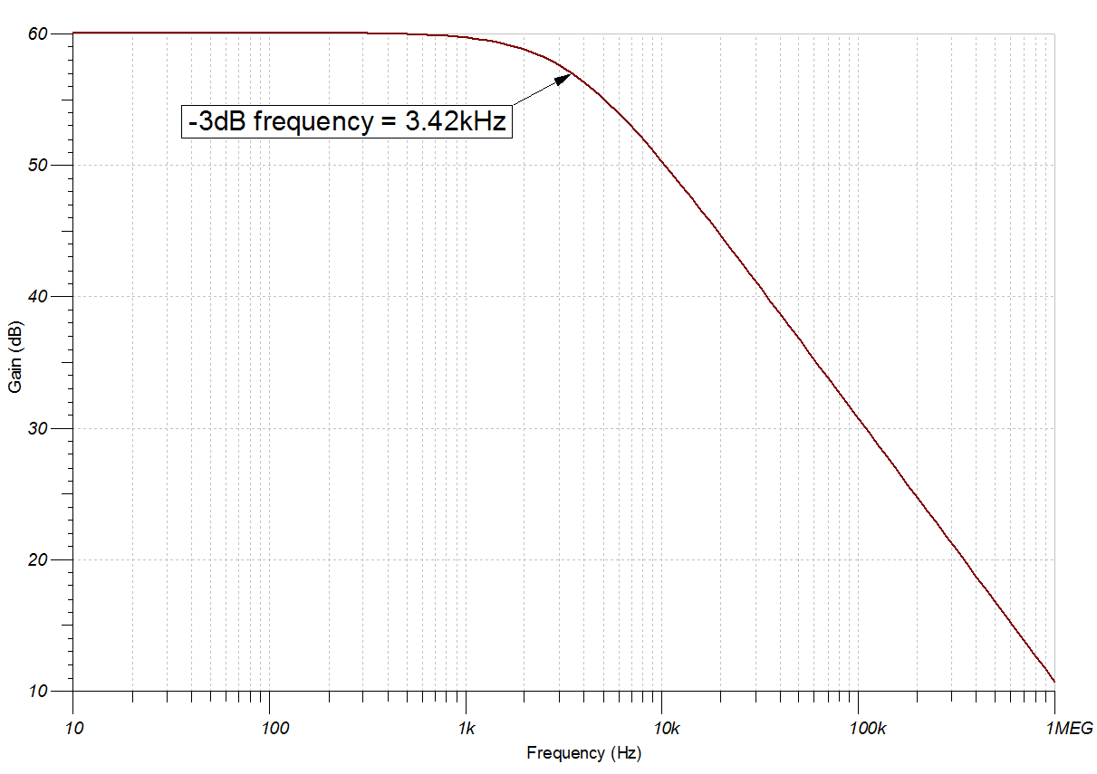
AC Simulation Results
The simulation is very close to the calculation.

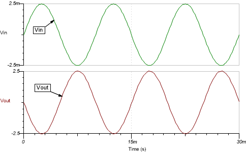
Transient Simulation Results

Design References
- See Analog Engineer's Circuit Cookbooks for the comprehensive TI circuit library.
- TI Precision Labs
- See the 1 MHz, Single-Supply, Photodiode Amplifier Reference Design.
Design Featured Op Amp
| OPA192 | |
|---|---|
| Vss | ±2.25V to ±18V |
| VinCM | Rail-to-Rail |
| Vout | Rail-to-Rail |
| Vos | 5µV |
| Iq | 1mA |
| Ib | 5pA |
| UGBW | 10MHz |
| SR | 20V/µs |
| #Channels | 1, 2, 4 |
| www.ti.com/product/OPA192 | |
Design Alternate Op Amp
| TLV9062 | |
|---|---|
| Vss | 1.8V to 5.5V |
| VinCM | Rail-to-Rail |
| Vout | Rail-to-Rail |
| Vos | 0.3mV |
| Iq | 538µA |
| Ib | 0.5pA |
| UGBW | 10MHz |
| SR | 6.5V/µs |
| #Channels | 1,2,4 |
| www.ti.com/product/TLV9062 | |