SLAAE41 September 2021 MSP430AFE221 , MSP430AFE222 , MSP430AFE223 , MSP430AFE231 , MSP430AFE232 , MSP430AFE233 , MSP430AFE251 , MSP430AFE252 , MSP430AFE253 , MSP430BT5190 , MSP430F1101 , MSP430F1101A , MSP430F1111A , MSP430F112 , MSP430F1121 , MSP430F1121A , MSP430F1122 , MSP430F1132 , MSP430F122 , MSP430F1222 , MSP430F123 , MSP430F1232 , MSP430F133 , MSP430F135 , MSP430F147 , MSP430F1471 , MSP430F148 , MSP430F1481 , MSP430F149 , MSP430F1491 , MSP430F155 , MSP430F156 , MSP430F157 , MSP430F1610 , MSP430F1611 , MSP430F1612 , MSP430F167 , MSP430F168 , MSP430F169 , MSP430F2001 , MSP430F2002 , MSP430F2003 , MSP430F2011 , MSP430F2012 , MSP430F2013
1 Add Housekeeping Functions to Your MSP430™ MCU: Power Sequencer
MSP430FR2433 provides a simple way to define power-on sequence of 4 power converters to meet user-defined system requirements. The MCU stays in low power mode and wakes up by a rising edge on Enable pin. On the easy-to-use graphical configuration GUI, users can detect the current sequence and modify it for the next time. Since the modified sequence is stored into FRAM, there is no worry about the loss of the data even after a power-off reset.
Implementation
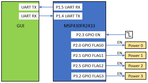
In this solution, the timers count at the clock of ACLK. It is sourced from the internal trimmed low-frequency REFO at the frequency of 32.768kHz. Pin P2.3 detects the enable signal and generates an interrupt to start the timers. The two timers with two comparators each are used to generate interrupts at every power-on moment. Users can modify the power-on moment by configurating the Timer_A Capture/Compare registers (TAxCCRn). Pins P2.0, P2.1, P2.5, P3.2 are used to generate the power-on signals. When the timer counts up to the value of a specified compare register, the corresponding pin outputs a high level. The power sequence can be detected and modified on host GUI by UART.
 Figure 1-1 Power Sequencer Block Diagram
Software Flow
Example code flow chart is shown as Figure 1-2. In the main program flow chart, after initialization and interrupt enabling, the microcontroller enters a low-power mode, and waits for interrupt requests triggered by peripheral events.
When the ENABLE interrupt comes from P2.3. The MCU starts the two timers and waits for Timer ISR. Meanwhile, the ENALBE LED on host is lit up.
When the timer counts up to value of TAxCCRn, the timer interrupt is raised. The corresponding output port is set to high and the corresponding LED on host is lit up. Meantime, the relevant slider indicates the time interval.
After all of the power converters are powered on. The total power-on sequence is shown on GUI.
Users can modify the sequence for the next time. The data is saved in FRAM, which will be applied to initiate the timers after reset.
 Figure 1-2 Example Code Software Flow
Development Environment
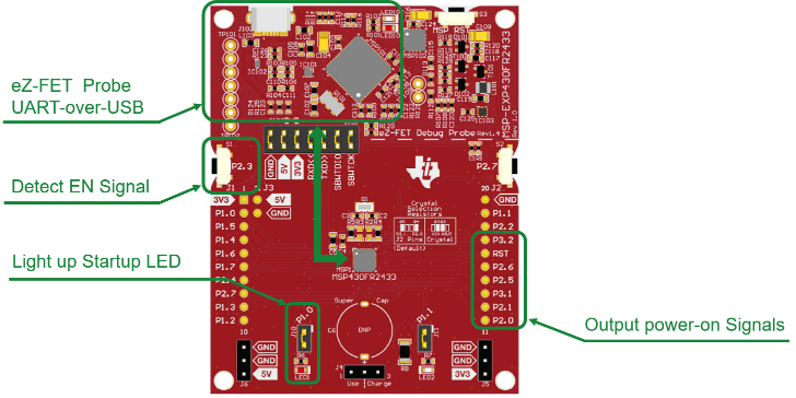
The MSP430FR2433 LaunchPad™ Development Kit can be used on this example project. Back-channel UART interface on eZ-FET of the LaunchPad can be used on UART communication with GUI. The COM channel number information can be found on the device management of the control panel. Port 1.0 is used to light up LED for the flag of startup. Port 2.3 is used to detect the enable signal. Port 2.0, 2.1, 2.5 and 3.2 are applied to output the power-on signals.
 Figure 1-3 MSP430FR2433 Lanuchpad
Performance
The GUI is used to show and modify the power-on sequence. The data is transmitted by UART on P1.5/UCA0RXD and P1.4/UCA0TXD. A baud rate of 9600 must be selected with one stop bit and no parity.
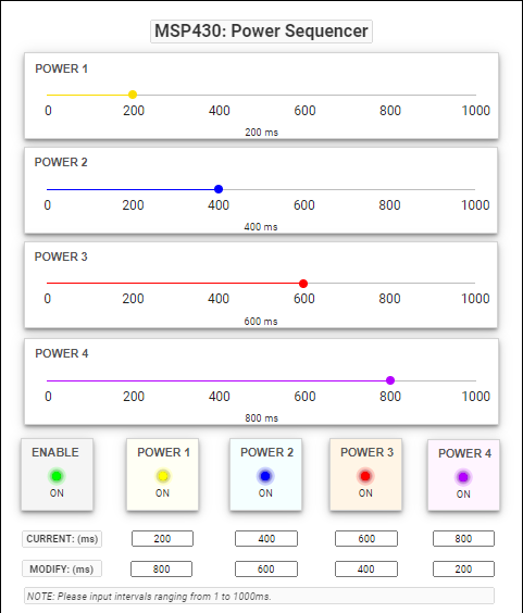
GUI interface is presented as Figure 1-4. On the top, there are four sliders which are used to indicate the time intervals. Below them are five LEDs. On the bottom of GUI, two row of text boxes are applied to detect and modify the sequence.
Once press the Reset switch on the LauncnPad, GUI is reset, including turning off LEDs and clearing all the data. Once press the button connected to P2.3 on the LauncnPad, the enable LED is lit up and the Timers start to count. When the Timer counts up to the power-on moment of POWERn, the corresponding LEDn on GUI is lit up. And the corresponding slider shows the time interval between the enable moment and power-on moment. After all LEDs are lit up, the total sequence is shown in the text boxes on the right of “CURRENT”. The power-on sequence of the next time can be modified in the text boxes on the right of “MODIFY”. Users can input the time interval ranging from 1 to 1000 milliseconds.
The size of code with GUI is 6492 bytes. The size of code without GUI is 2676 bytes. The average power consumption of the programmable system waiting for enable signals is around 20μA. It is dominated by the LPM3 current of the device.
 Figure 1-4 Power Sequencer GUI
To Get Started
1. Watch the training video “Power Sequencer with a Housekeeping MCU” to learn how to use the GUI to configurate a power-on sequence.
2. Order a MSP430FR2433 LaunchPad kit to evaluate the Power Sequencer example code.
3. Download and test this example with the Power Sequencer example GUI to receive the power sequence and modify it simply.
4. Evaluate the Power Sequencer example code for the MSP430FR2433 LaunchPad kit.
Device Recommendations
The device used in this example is part of the MSP430 housekeeping portfolio. This example can be used with the devices shown in Table 1Table 1 with minimal code changes.
| Part Number | Key Features |
| MSP430FR2433 | 16KB FRAM, 4KB SRAM, 10-bit ADC, UART/SPI/I2C, Timer |
| MSP430FR2422 | 8KB FRAM, 2KB SRAM, 10-bit ADC, UART/SPI/I2C, Timer |