SLAS411D November 2004 – February 2016 DAC8811
PRODUCTION DATA.
- 1 Features
- 2 Applications
- 3 Description
- 4 Revision History
- 5 Device Comparison Table
- 6 Pin Configuration and Functions
- 7 Specifications
- 8 Detailed Description
- 9 Application and Implementation
- 10Power Supply Recommendations
- 11Layout
- 12Device and Documentation Support
- 13Mechanical, Packaging, and Orderable Information
1 Features
- ±0.5 LSB DNL
- 16-Bit Monotonic
- ±1 LSB INL
- Low Noise: 12 nV/√Hz
- Low Power: IDD = 2 µA
- 2.7-V to 5.5-V Analog Power Supply
- 2-mA Full-Scale Current ±20%,
with VREF = 10 V - 50-MHz Serial Interface
- 0.5-μs Settling Time
- 4-Quadrant Multiplying Reference
- Reference Bandwidth: 10 MHz
- ±10-V Reference Input
- Reference Dynamics: –105 THD
- Tiny 8-Lead 3 × 3 mm VSON and 3 × 5 mm VSSOP Packages
- Industry-Standard Pin Configuration
2 Applications
- Automatic Test Equipment
- Instrumentation
- Digitally Controlled Calibration
- Industrial Control PLCs
3 Description
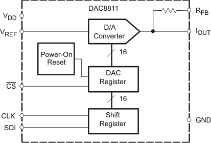
The DAC8811 multiplying digital-to-analog converter (DAC) is designed to operate from a single 2.7-V to 5.5-V supply.
The applied external reference input voltage VREF determines the full-scale output current. An internal feedback resistor (RFB) provides temperature tracking for the full-scale output when combined with an external I-to-V precision amplifier.
A serial data interface offers high-speed, three-wire microcontroller-compatible inputs using data-in (SDI), clock (CLK), and chip-select (CS).
On power-up, the DAC register is filled with zeroes, and the DAC output is at zero scale.
The DAC8811 is packaged in space-saving 8-lead VSON and VSSOP packages.
Device Information(1)
| PART NUMBER | PACKAGE | BODY SIZE (NOM) |
|---|---|---|
| DAC8811 | VSSOP (8) | 3.00 mm × 3.00 mm |
| VSON (8) | 3.00 mm × 3.00 mm |
- For all available packages, see the orderable addendum at the end of the datasheet.
