SLLA479 March 2020 ISO7741E-Q1
For automotive applications, Controller Area Network Flexible Data Rate (CAN FD) has become the de facto standard for most automakers. Unquestionably, the higher speed of CAN FD over Classical CAN enables faster communication of data allowing for more bandwidth, lower latency for the messages, or increased nodes on the CAN bus. Additionally, if the CAN communication is used between different voltage domains as in hybrid electric vehicles (HEVs) and electric vehicles (EVs), digital isolators are often used to help with protection of the low-voltage side from high-voltage side and improve noise immunity.
The CAN protocol is preferred in automotive applications due to its prioritization and arbitration features, making it popular in time-critical applications, such as belt starter generators, traction inverters, battery management systems. Hence the timing specifications of the CAN device become critical when selecting the right device for your system. Table 1-1 shows the main specifications to consider when designing a system that meets the physical layer requirements of the ISO 11898-2:2016 high-speed CAN specification.
| Parameter | MIN | MAX | |
|---|---|---|---|
| tPROP(LOOP1) | Total loop delay, driver input (TXD) to receiver output (RXD), recessive to dominant | 255 ns | |
| tPROP(LOOP2) | Total loop delay, driver input (TXD) to receiver output (RXD), dominant to recessive | 255 ns | |
| tBIT(BUS) | Bit time on CAN bus output pins with tBIT(TXD) = 500 ns (for 2 Mbps CAN FD) | 435 ns | 530 ns |
| Bit time on CAN bus output pins with tBIT(TXD) = 200 ns (for 5 Mbps CAN FD) | 155 ns | 210 ns | |
| tBIT(RXD) | Bit time on RXD output pins with tBIT(TXD) = 500 ns (for 2 Mbps CAN FD) | 400 ns | 550 ns |
| Bit time on RXD output pins with tBIT(TXD) = 200 ns (for 5 Mbps CAN FD) | 120 ns | 220 ns | |
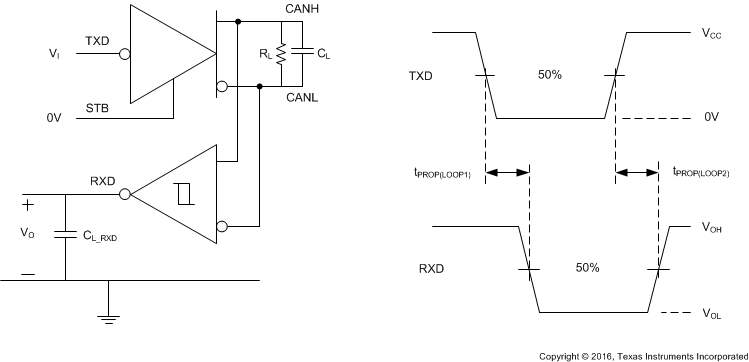
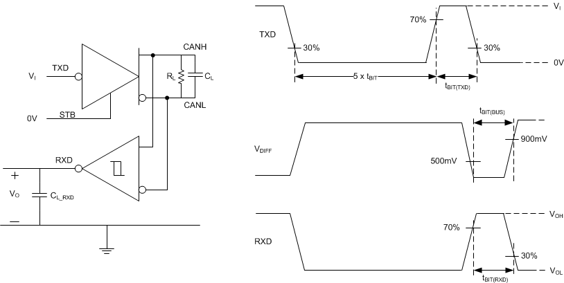
Figure 1-1 and Figure 1-2 show the test setup for the measurement of these parameters for the CAN transceiver by itself. Figure 1-1 shows the measurement of the total loop delay from the driver input (TXD) to receiver output (RXD). This measurement is done in the recessive to dominant state as shown by tPROP(LOOP1) and the dominant to recessive state as shown by tPROP(LOOP2). Figure 1-2 measures the variation in the bit width as it propagates through the transmitter to the output and back through the receiver to the receiver output.
 Figure 1-1 tPROP(LOOP)Test
Circuit and Measurement
 Figure 1-2 CAN FD Bit Timing Parameter
Measurement
Figure 1-2 CAN FD Bit Timing Parameter
MeasurementCAN devices such as the Grade 0 CAN FD transceiver TCAN1044EV-Q1 can meet the requirements over the temperature range of -40 °C to 150 °C as shows in Table 1-2 .
| ISO 11898-2:2016 | TCAN1044EV-Q1 | |||
|---|---|---|---|---|
| Parameter | MIN | MAX | MIN | MAX |
| tPROP(LOOP1) | 255 ns | 210 ns | ||
| tPROP(LOOP2) | 255 ns | 210 ns | ||
tBIT(BUS)
2 Mbps CAN FD | 435 ns | 530 ns | 460 ns | 510 ns |
tBIT(BUS)
5 Mbps CAN FD | 155 ns | 210 ns | 160 ns | 210 ns |
tBIT(RXD)
2 Mbps CAN FD | 400 ns | 550 ns | 445 ns | 515 ns |
tBIT(RXD)
5 Mbps CAN FD | 120 ns | 220 ns | 145 ns | 215 ns |
For applications that require isolation between the CAN transceiver and the microcontroller, simply looking at the CAN transceiver timing performance is not enough. It is important to add the timing performance of the digital isolator that is in series with the CAN transceiver to ensure the two-chip solution still meets the timing specification. Isolator datasheets provide the propagation delay and pulse width distortion specifications.
For example, these timing specifications for the Grade 0 ISO7741E-Q1 are shown in Table 1-3:
| ISO7741E-Q1 (-40 °C to +150 °C) | |||
|---|---|---|---|
| Parameter | MIN | MAX | |
| tPLH, tPHL | Propagation delay time | 6 ns | 16.5 ns |
| PWD | Pulse width distortion |tPHL – tPLH| | 4.9 ns | |
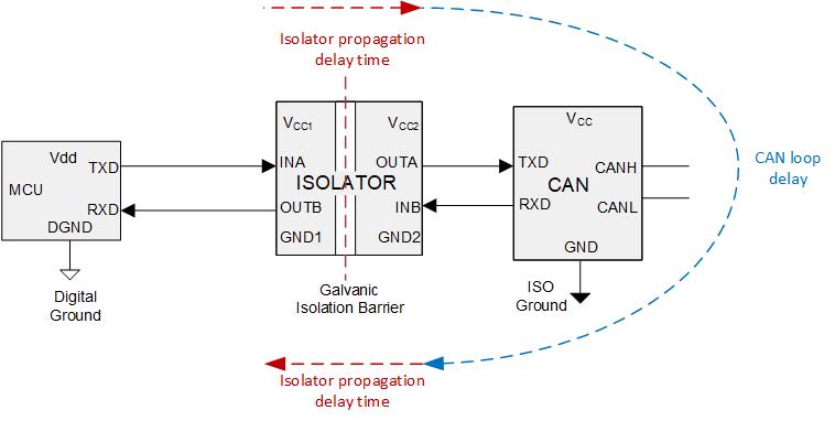
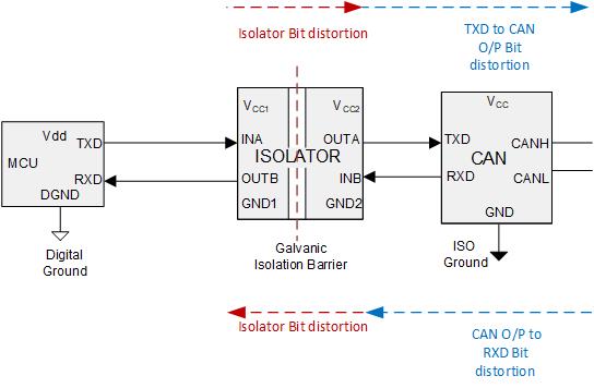
Based on the individual timing specifications for the digital isolator and the CAN transceiver, the combined data can be calculated as follows (as shown in Figure 1-3 and Figure 1-4):
Total loop delay from the driver input to the receiver output: CAN loop delay + 2 x Isolator propagation delay time
 Figure 1-3 Total loop delay for isolated CAN system
Minimum bit time on the bus output pins = Minimum CAN tBIT(BUS) time -Maximum Isolator pulse width distortion. Maximum bit time on the bus output pins = Maximum CAN tBIT(BUS) time + Maximum Isolator pulse width distortion. Minimum bit time on the receiver output pins = Minimum CAN tBIT(RXD) time - 2 x Maximum Isolator pulse width distortion. Maximum bit time on the receiver output pins = Maximum CAN tBIT(RXD) time + 2 x Maximum Isolator pulse width distortion.
 Figure 1-4 Total bit time for isolated
CAN
Figure 1-4 Total bit time for isolated
CANBased on the formulae discussed above, the combined timing specifications of the two-chip isolated CAN solution is shown in Table 1-4.
| ISO 11898-2:2016 | ISO7741E-Q1 + TCAN1044EV-Q1 (-40 °C to +150 °C) | |||
|---|---|---|---|---|
| Parameter | MIN | MAX | MIN | MAX |
| tPROP(LOOP1) | 255 ns | 243 ns | ||
| tPROP(LOOP2) | 255 ns | 243 ns | ||
tBIT(BUS)
2 Mbps CAN FD | 435 ns | 530 ns | 455.1 ns | 514.9 ns |
tBIT(BUS)
5 Mbps CAN FD | 155 ns | 210 ns | 155.1 ns | 214.9 ns |
tBIT(RXD)
2 Mbps CAN FD | 400 ns | 550 ns | 435.2 ns | 524.8 ns |
tBIT(RXD)
5 Mbps CAN FD | 120 ns | 220 ns | 135.2 ns | 224.8 ns |
From the table it is clear that the Grade 0 isolator ISO7741E-Q1 when used along with the Grade 0 CAN FD transceiver TCAN1044EV-Q1, can meet the ISO 11898-2:2016 specifications up to CAN FD speed for 2 Mbps.
This article discussed the key timing specs and calculation examples to determine if the chosen discrete isolator and CAN transceiver can meet the CAN standards. Selecting the right components upfront will ensure the proper CAN system operation and speed up release to production.