SLOS836E May 2013 – June 2016 TAS5729MD
PRODUCTION DATA.
- 1 Features
- 2 Applications
- 3 Description
- 4 Revision History
- 5 Related Devices
- 6 Pin Configuration and Functions
-
7 Specifications
- 7.1 Absolute Maximum Ratings
- 7.2 ESD Ratings
- 7.3 Recommended Operating Conditions
- 7.4 Thermal Information
- 7.5 Digital I/O Pins
- 7.6 Master Clock
- 7.7 Serial Audio Port
- 7.8 Protection Circuitry
- 7.9 Speaker Amplifier in All Modes
- 7.10 Speaker Amplifier in Stereo Bridge Tied Load (BTL) Mode
- 7.11 Speaker Amplifier in Stereo Post-Filter Parallel Bridge Tied Load (Post-Filter PBTL) Mode
- 7.12 Headphone Amplifier and Line Driver
- 7.13 Reset Timing
- 7.14 I2C Control Port
- 7.15 Typical Electrical Power Consumption
- 7.16 Typical Characteristics
- 8 Parameter Measurement Information
-
9 Detailed Description
- 9.1 Overview
- 9.2 Functional Block Diagram
- 9.3 Feature Description
- 9.4 Device Functional Modes
- 9.5 Programming
- 9.6
Register Maps
- 9.6.1 Clock Control Register (0x00)
- 9.6.2 Device ID Register (0x01)
- 9.6.3 Error Status Register (0x02)
- 9.6.4 System Control Register 1 (0x03)
- 9.6.5 Serial Data Interface Register (0x04)
- 9.6.6 System Control Register 2 (0x05)
- 9.6.7 Soft Mute Register (0x06)
- 9.6.8 Volume Registers (0x07, 0x08, 0x09)
- 9.6.9 Volume Configuration Register (0x0E)
- 9.6.10 Modulation Limit Register (0x10)
- 9.6.11 Interchannel Delay Registers (0x11, 0x12, 0x13, and 0x14)
- 9.6.12 PWM Shutdown Group Register (0x19)
- 9.6.13 Start/Stop Period Register (0x1A)
- 9.6.14 Oscillator Trim Register (0x1B)
- 9.6.15 BKND_ERR Register (0x1C)
- 9.6.16 Input Multiplexer Register (0x20)
- 9.6.17 Channel 4 Source Select Register (0x21)
- 9.6.18 PWM Output MUX Register (0x25)
- 9.6.19 AGL Control Register (0x46)
- 9.6.20 PWM Switching Rate Control Register (0x4F)
- 9.6.21 EQ Control (0x50)
-
10Application and Implementation
- 10.1 Application Information
- 10.2
Typical Applications
- 10.2.1 Stereo BTL Configuration With Headphone and Line Driver Amplifier
- 10.2.2 Mono PBTL Configuration with Headphone and Line Driver Amplifier
- 11Power Supply Recommendations
- 12Layout
- 13Device and Documentation Support
- 14Mechanical, Packaging, and Orderable Information
1 Features
- Audio I/O Configuration:
- Audio Digital Signal Processing:
- Digital Equalization
- Two-Band Automatic Gain Limiting
- Coarse and Fine Volume Control
- PWM Level Meter
- General Operational Features:
- Audio Performance (PVDD = 18 V, RLOAD = 8 Ω)
- Idle Channel Noise = 56 µVrms
- THD+N at 1 W, 1 kHz, = 0.15%
- SNR = 105 dB (reference to 0 dBFS)
2 Applications
- LCD/LED TV and Multipurpose Monitors
- Sound Bars, Docking Stations, PC Audio
- Consumer Audio Equipment
3 Description
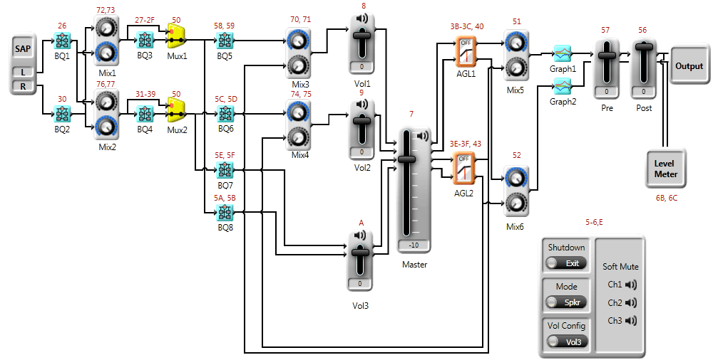
The TAS5729MD is a stereo I²S input device which includes a digital auto processor with two-band automatic gain limiting (AGL), digital equalization, course and fine volume control, and PWM level meter. The AGL is an enhanced dynamic range compression (DRC) function. The device can operate from a wide PVDD power supply range to enable use in numerous applications. The TAS5729MD operates with a nominal supply voltage from 4.5 to 24 VDC. The device is controlled by an I²C control port. The device has an integrated DirectPath™ headphone amplifier and line driver to increase system-level integration and reduce total solution costs.
An optimal mix of thermal performance and device cost is provided in the 200-mΩ RDS(ON) of the output MOSFETs. Additionally, a thermally enhanced HTSSOP provides excellent operation in the elevated ambient temperatures found in today's modern consumer electronic devices.
The entire TAS5729xx family is pin-to-pin compatible allowing a single hardware solution to be used across several end application platforms. Additionally, the I²C register map in the entire TAS5729xx family is identical to ensure low development overhead to choose between devices based upon system level requirements.
Device Information(1)
| PART NUMBER | PACKAGE | BODY SIZE (NOM) |
|---|---|---|
| TAS5729MD | HTSSOP (48) | 12.50 mm × 6.10 mm |
- For all available packages, see the orderable addendum at the end of the data sheet.
Signal Processing Flow

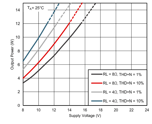
Power at 10% THD+N vs PVDD

NOTE:
Dashed lines represent thermally limited region.