SLUSAP5A December 2011 – November 2016 TPS53316
PRODUCTION DATA.
- 1 Features
- 2 Applications
- 3 Description
- 4 Revision History
- 5 Pin Configuration and Functions
- 6 Specifications
- 7 Detailed Description
- 8 Application and Implementation
- 9 Power Supply Recommendations
- 10Layout
- 11Device and Documentation Support
- 12Mechanical, Packaging, and Orderable Information
1 Features
- 96% Maximum Efficiency
- Continuous 5-A Output Current Capability
- Support all MLCC Output Capacitor
- SmoothPWM™ Auto-Skip Eco-Mode™ for Light-Load Efficiency
- Voltage Mode Control
- Single Rail Input
- Selectable Frequency
- Selectable OCP Threshold
- Selectable Soft-Start Time
- 2.9-V to 6-V Input Voltage Range
- Adjustable Output Voltage Ranging from 0.6 V up to 0.8 × VIN
- Soft-Stop Output Discharge During Disable
- Overcurrent, Overvoltage, and Overtemperature Protection
- Open-Drain Power Good Indication
- Internal Bootstrap Switch
- Supports Prebias Start-Up Functionality
- Small 3 mm × 3 mm, 16-Pin, QFN Package
- Low RDS(on), 22-mΩ With 3.3-V Input and 18-mΩ With 5-V Input
2 Applications
- Low-Voltage Applications for 5-V Step-Down Rails
- Low-Voltage Applications for 3.3-V Step-Down Rails
3 Description
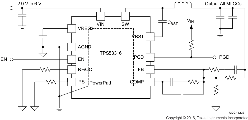
The TPS53316 device provides a fully integrated 3.3-V or 5-V input, synchronous buck converter with 16 total components, in 200 mm2 of PCB area. Due to low RDS(on) and TI proprietary SmoothPWM skip mode of operation, it enables 96% peak efficiency, and over 90% efficiency at load as light as 100 mA. It requires only two 22-µF ceramic output capacitors for a power-dense, 5-A solution.
TPS53316 features 750-kHz, 1.1-MHz, and 2-MHz switching frequency selections, prebias start-up, selectable internal softstart, output soft discharge, internal VBST switch, power good, EN/Input UVLO, overcurrent, overvoltage, undervoltage, and overtemperature protections and all ceramic output capacitor support. It supports input voltages from
2.9 V to 6 V, and no extra bias voltage is needed. The output voltage is adjustable from 0.6 V up to
0.8 × VIN.
TPS53316 is available in the 3 mm × 3 mm, 16-pin QFN package (Green RoHs compliant and Pb free) and is specified from –40°C to 85°C.
Device Information(1)
| PART NUMBER | PACKAGE | BODY SIZE (NOM) |
|---|---|---|
| TPS53316 | QFN (16) | 3.00 mm × 3.00 mm |
- For all available packages, see the orderable addendum at the end of the data sheet.
Typical Application Circuit
