SLVS815D January 2008 – October 2016 TPS62560 , TPS62561 , TPS62562
PRODUCTION DATA.
- 1 Features
- 2 Applications
- 3 Description
- 4 Revision History
- 5 Device Comparison Table
- 6 Pin Configuration and Functions
- 7 Specifications
- 8 Detailed Description
- 9 Application and Implementation
- 10Power Supply Recommendations
- 11Layout
- 12Device and Documentation Support
- 13Mechanical, Packaging, and Orderable Information
1 Features
- Output Current up to 600 mA
- Input Voltage Range from 2.5 V to 5.5 V
- Output Voltage Accuracy in PWM Mode ±2.5%
- Typical 15-μA Quiescent Current
- 100% Duty Cycle for Lowest Dropout
- Soft Start
- Available in a Small SOT, and
2 mm × 2 mm × 0.8 mm SON Package - For Improved Features Set, See the TPS62290 device (SLVS764)
2 Applications
- PDAs, Pocket PCs, Portable Media Players
- Low-Power DSP Supply
- Point-of-Load (POL) Applications
3 Description
The TPS62560 device is a high efficiency synchronous step down converter, optimized for battery powered portable applications. It provides up to 600-mA output current from batteries, such as single Li-Ion or other common chemistry AA and AAA cells.
With an input voltage range of 2.5 V to 5.5 V, the device is targeted to power a large variety of portable handheld equipment or POL applications.
The TPS62560 family operates at 2.25-MHz fixed switching frequency and enters a Power Save Mode operation at light load currents to maintain a high efficiency over the entire load current range.
The Power Save Mode is optimized for low output voltage ripple. For low noise applications, the device can be forced into fixed frequency PWM mode by pulling the MODE pin high. In the shutdown mode the current consumption is reduced to less than 1 µA. The TPS62560 allows the use of small inductors and capacitors to achieve a small solution size.
TPS62560 and TPS62562 are available in a 2-mm × 2-mm, 6-pin SON package, whereas the TPS62561 is available in a 5-pin SOT package.
Device Information(1)
| PART NUMBER | PACKAGE | BODY SIZE (NOM) |
|---|---|---|
| TPS62560, TPS62562 | SON (6) | 2.00 mm × 2.00 mm |
| TPS62561 | SOT (5) | 2.90 mm × 1.60 mm |
- For all available packages, see the orderable addendum at the end of the data sheet.
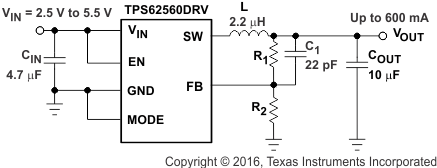
Typical Application Schematic

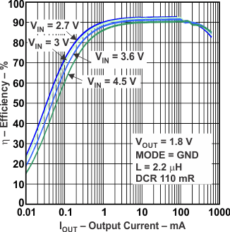
Efficiency vs Output Current
