TIDT225 March 2021
1 Description
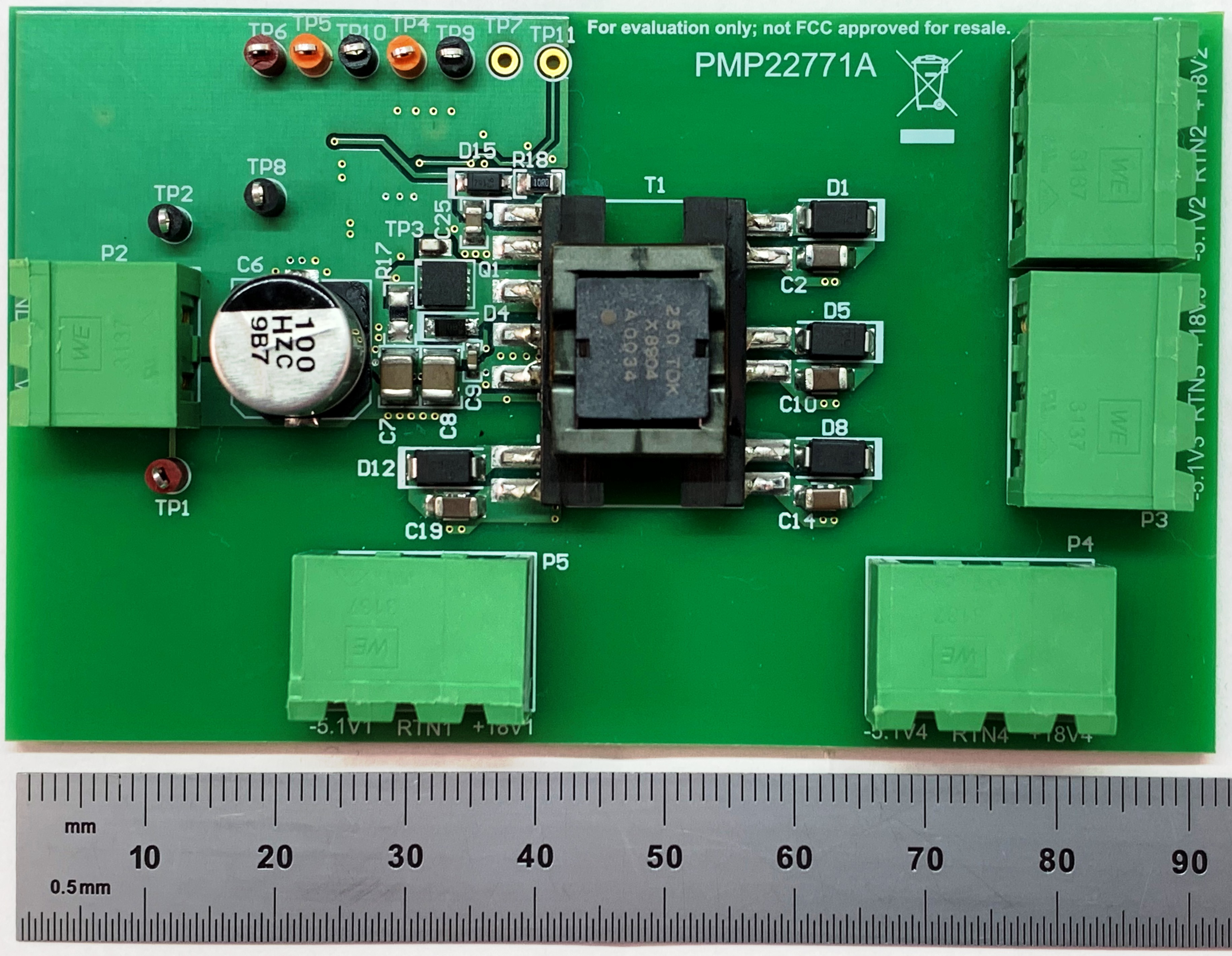
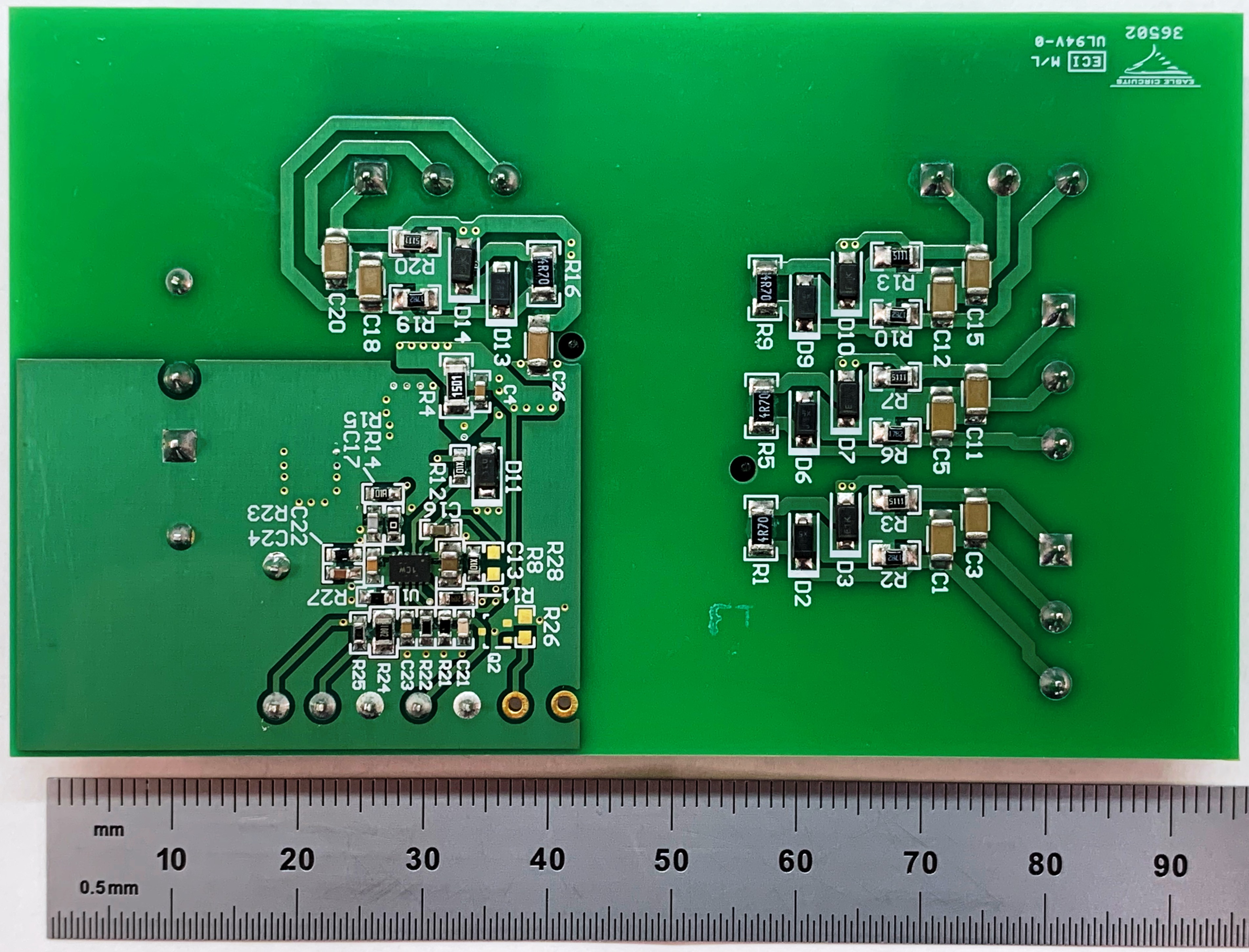
This isolated primary regulated flyback converter provides a total of eight output voltages. These outputs consist of four isolated pairs of +18-V and –5.1-V outputs, with three pairs capable of 25 mA maximum for and one capable of 75 mA maximum. These outputs are designed to be used as an IGBT driver bias supply for a total of six IGBTs (25 mA for three high-side drivers and 75 mA for three low-side drivers). It operates over an input voltage range of 7 V–32 V in a compact form factor with a single transformer.
 Figure 1-1 Top of PCB
 Figure 1-2 Bottom of PCB