10s–16s Battery Pack Reference Design With Accurate Cell Measurement and High-Side MOSFET Control
Description
This reference design is a low standby and ship-mode current consumption and high cell voltage accuracy 10s–16s Lithium-ion (Li-ion), LiFePO4 battery pack design. It monitors each cell voltage, pack current, cell and MOSFET temperature with high accuracy and protects the Li-ion, LiFePO4 battery pack against cell overvoltage, cell undervoltage, overtemperature, charge and discharge over current and discharge short-circuit situations. It adopts high-side N-channel MOSFET architecture and has strong driving on and off capability. Through an efficient auxiliary power supply strategy, this reference design achieves 100-μA stand-by and 10-μA ship mode consumption, saving more energy and allowing longer shipping time and idle time. These features make this reference design highly applicable for e-bike and e-scooter battery pack applications.
Resources
| TIDA-010208 | Design Folder |
| BQ76952, BQ77216, MSP430FR2155 | Product Folder |
| LM5163, TCAN1042HV, TCAN1044V | Product Folder |
| TLV704, TMP61 | Product Folder |

Features
Ultra-low current consumption:
-
Typical 100-μA when in standby mode
-
Typical 10-μA when in shipping mode
-
High cell voltage accuracy without calibrations:
-
±5 mV at 25°C; ±10 mV at 0°C–60°C; ±15 mV at –40°C to 85°C
-
Robust battery cell protection, including:
-
Primary: cell overvoltage, cell undervoltage, two levels overcurrent discharge, overcurrent charge, discharge short circuit and overtemperature
-
Secondary: cell over voltage, cell undervoltage and overtemperature
-
Other system protections, including: cell open wire and host watchdog
Support random cell connections
Reverse charger and high voltage on PACK side
High-side N-channel MOSFETs and strong driving capability
Applications
Battery pack – e-bike, e-scooter, LEV
Other industrial battery pack (≥ 10s)
1 System Description
The e-bike market is growing rapidly. Because of the weight limited and longer endurance needs, the battery cell chemistry of the battery pack is shifting from Lead-acid to Li-ion, Li-polymer, or Li-iron phosphate types. This chemistry is good in both volumetric and gravimetric energy density. While this chemistry provides high energy density and thereby lower volume and weight as an advantage, they are associated with safety concerns and need more accurate and complicated monitoring and protections. Those concerns are cell undervoltage (CUV) and cell overvoltage (COV), overtemperature (OT), both overcurrent in charge (OCC) and discharge (OCD), and short-circuit discharge (SCD), all of which contribute to the accelerating cell degradation and may lead to thermal runaway and explosion. Therefore the pack current, cell temperature, and each cell voltage should be monitored timely in case of some unusual situations. The battery pack must be protected against all these situations.
Good measurement accuracy is always required, especially the cell voltage, pack current, and cell temperature. Precision is necessary for accurate protections and battery pack state of charge (SoC) calculations. This is especially true for LiFePO4 battery pack applications because of the flat voltage. Another important feature for battery-powered applications is the current consumption, especially when in ship mode or standby mode. Lower current consumption saves more energy and gives longer storage time without over discharging the battery.
This design focuses on e-bike or e-scooter battery pack applications and is also suitable for other high-cell applications, such as a mowing robot battery pack, 48-V family energy storage system battery packs, and so forth. It contains both primary and secondary protections to ensure safe use of the battery pack. The primary protection protects the battery pack against all unusual situations, including: cell overvoltage, cell undervoltage, overtemperature, overcurrent in charge and discharge, and short-circuit discharge. The secondary protection which supports independent cell overvoltage protection, cell undervoltage protection, and overtemperature protection is an add-on board and is easily removed and added based on actual demands. It achieves within ±5-mV cell voltage measurement accuracy at 25°C and ±10 mV at 0°C to 60°C without any further calibrations. This solution carefully designs the auxiliary power architecture, which achieves quite low ship mode (10 μA) and standby mode (100 μA) current consumption with a limited number of components and simple control strategy.
2 System Overview
Table 2-1 lists the key system specifications of this design.
| Parameter | Conditions | Spec Range | Unit | ||
|---|---|---|---|---|---|
| Minimum | Typical | Maximum | |||
| Cell architecture | BQ76942 | 3 | 10 | Series | |
| BQ769142 | 3 | 14 | Series | ||
| BQ76952 | 3 | 16 | Series | ||
| Cell balancing peak current | Cell voltage: 4000 mV | 117 | mA | ||
| Charge current | 27 | A | |||
| Discharge current | 27 | A | |||
| Pre-discharge current | Pack voltage: 48 V | 160 | mA | ||
| Cell Voltage accuracy | 25°C | ±5 | mV | ||
| 0°C–60°C | ±10 | mV | |||
| Pack current accuracy | < 2 A | ±10 | mA | ||
| > 2 A | ±0.5 | % | |||
| Primary OV protection | Threshold | 4200 | mV | ||
| Delay | 2 | s | |||
| Secondary OV protection | Threshold | 4325 | mV | ||
| Delay | 1 | s | |||
| Primary UV protection | Threshold | 2530 | mV | ||
| Delay | 2 | s | |||
| Secondary UV protection | Threshold | 2250 | mV | ||
| Delay | 1 | s | |||
| OCD protection - level 1 | Threshold | 10 | A | ||
| Delay | 425 | ms | |||
| OCD protection - level 2 | Threshold | 30 | A | ||
| Delay | 56 | ms | |||
| OCC protection | Threshold | 10 | A | ||
| Delay | 425 | ms | |||
| SCD protection | Threshold | 200 | A | ||
| Delay | 300 | µs | |||
| Over temperature protection | Charge | 55 | °C | ||
| Discharge | 60 | °C | |||
| Under temperature protection | Charge | 0 | °C | ||
| Discharge | –20 | °C | |||
| Maximum pack+ voltage | Charge MOSFET off | 120 | V | ||
| Standby mode current consumption | 100 | µA | |||
| Ship mode current consumption | 10 | µA | |||
2.1 Block Diagram
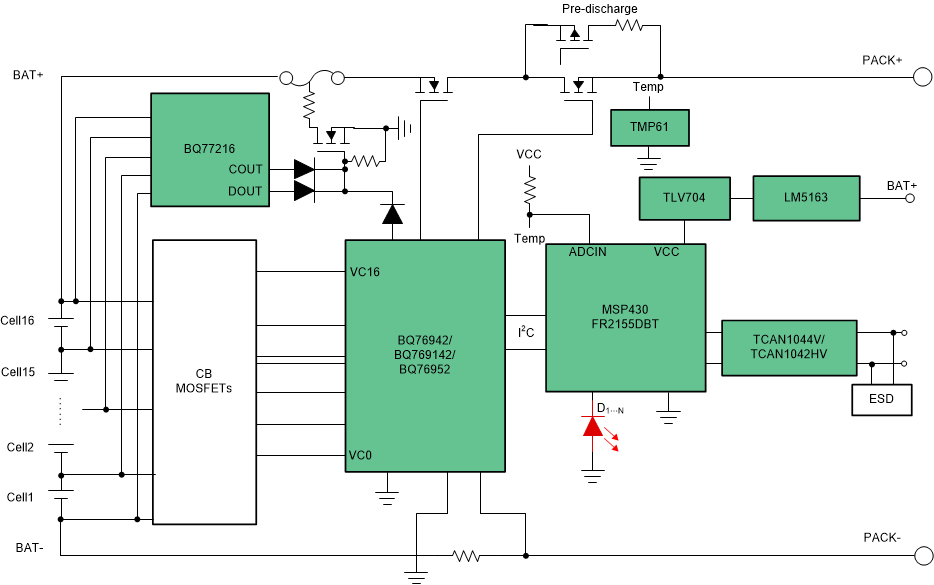
Figure 2-1 shows the system diagram. It uses the high-accuracy battery monitor and protector bq769x2 family from TI to monitor each cell voltage, pack current and temperature data, and protect the battery pack from all unusual situations, including: COV, CUV, OT, overcurrent in charge and discharge and short-circuit discharge. It has 3 devices: bq76942 to cover 3s to 10s applications, bq769142 to cover up to 14s applications, and bq76952 to cover up to 16s applications. They are pin-to-pin devices, which makes it very easy to update the design to match different battery cell applications with a limited number of component changes. This design uses an independent 16s secondary protector bq77216 for voltage and temperature protection. This helps the design pass some safety regulations without requiring an MCU to carry out protection work, which saves the safety certifications of the firmware. There is a lower-power MSP430TM MCU MSP430FR2155 which will communicate with the monitor, deal with all system control strategy, and upload all the requested information to the system side. This design has a CAN transceiver TCAN1044V or TCAN1042HV which both integrate level translation via the VIO terminal to allow for interfacing the transceiver IOs directly to 1.8-V, 2.5-V, 3.3-V, or 5-V logic IOs. The TCAN1044V has ±58-V bus fault protection voltage which is good enough to cover 36-V battery packs for e-assisted bikes or e-scooters. The TCAN1042HV is also recommended for 48-V ebike battery packs since it supports as high as ±70-V bus fault protection voltage. Since the MSP430FR2155 does not have an integrated CAN controller, CAN communication is not supported by this design. This design uses a 100-V input, 0.5-A, ultra-low IQ synchronous Buck DC/DC converter LM5163 with a low IQ LDO TLV704 as the auxiliary power. A ±1%, 10-kΩ linear thermistor with positive temperature coefficient and 0603 package TMP61 is utilized to monitor the MOSFET temperature and measured by MCU ADC.
Figure 2-1 TIDA-010208 Block
Diagram. 2.2 Design Considerations
Auxiliary Power Strategy
With the requests of low current consumption in standby mode and ship mode, this design uses the auxiliary power strategy shown in Figure 2-2.
 Figure 2-2 Auxiliary Power Strategy.
 The design has a 100-V Input, 0.5-A, ultra-low IQ synchronous Buck DC/DC converter LM5163 with a low IQ LDO TLV704 as the main power source when the system is working in normal mode. The BQ76952 regulator is configured to 5-V output which is the power source when the system is working in standby mode. The series diode on the BQ76952 regulator output makes sure all power is from the DC/DC converter in normal mode preventing the BQ76952 regulator circuits from overheating, so DC/DC output should be designed a little higher than 5 V, BQ76952 regulator output. Detailed component design guidance is available from the LM5163 and LM5164 converter quickstart design tool. When the system experiences a serious cell under voltage and must enter ship mode, the MCU will configure the BQ76952 device to enter shutdown mode through an I2C command or RST_SHUT PIN and turn off LM5163 output through the EN PIN, which configures the system to very low current consumption mode. This design supports both charger attach and system detect wake up functions. Both methods wake up the BQ76952 device and enable normal 5-V regulator output, then the MCU is powered on and will enable the LM5163 through the EN PIN. The whole system then returns to normal mode.
2.3 Highlighted Products
BQ76952
The BQ76952 device is a highly integrated, high-accuracy battery monitor and protector for 3-series to 16-series Li-Ion, Li-Polymer, and LiFePO4 battery packs. The device includes a high-accuracy monitoring system, a highly configurable protection subsystem, and support for autonomous or host controlled cell balancing. Integration includes high-side charge-pump NFET drivers, dual programmable LDOs for external system use, and a host communication peripheral supporting 400-kHz I2C, SPI, and HDQ one-wire standards. The BQ76952 device is available in a 48-pin TQFP package.
BQ77216
The BQ77216 family of products provides a range of voltage and temperature monitoring including overvoltage (OVP), undervoltage (UVP), open wire (OW), and overtemperature (OT) protection for li-ion battery pack systems. Each cell is monitored independently for overvoltage, undervoltage, and open-wire conditions. With the addition of an external NTC thermistor, the device can detect overtemperature conditions. In the BQ77216 device, an internal delay timer is initiated upon detection of an overvoltage, undervoltage, open-wire, or overtemperature condition. Upon expiration of the delay timer, the respective output is triggered into its active state (either high or low, depending on the configuration). The overvoltage triggers the COUT pin if a fault is detected, and undervoltage triggers the DOUT pin if a fault is detected. If an overtemperature or open-wire fault is detected, then both the DOUT and COUT will be triggered. For quicker production-line testing, the BQ77216 device provides a Customer Test Mode (CTM) with greatly reduced delay time.
LM5163
The LM5163 synchronous buck converter is designed to regulate over a wide input voltage range, minimizing the need for external surge suppression components. A minimum controllable on-time of 50 ns facilitates large step-down conversion ratios, enabling the direct step-down from a 48-V nominal input to low-voltage rails for reduced system complexity and solution cost. The LM5163 operates during input voltage dips as low as 6 V, at nearly 100% duty cycle if needed, making it an excellent choice for wide input supply range industrial and high cell count battery pack applications. With integrated high-side and low-side power MOSFETs, the LM5163 delivers up to 0.5-A of output current. A constant on-time (COT) control architecture provides nearly constant switching frequency with excellent load and line transient response. Additional features of the LM5163 include ultra-low IQ and diode emulation mode operation for high light-load efficiency, innovative peak and valley overcurrent protection, integrated VCC bias supply and bootstrap diode, precision enable and input UVLO, and thermal shutdown protection with automatic recovery. The LM5163 is available in a thermally-enhanced, 8- pin SO PowerPAD™ package.
TCAN1044V
The TCAN1044V is a high speed controller area network (CAN) transceiver that meets the physical layer requirements of the ISO 11898-2:2016 high-speed CAN specification. The TCAN1044V transceiver supports both classical CAN and CAN FD networks up to 8 megabits per second (Mbps). The TCAN1044V includes internal logic level translation via the VIO terminal to allow for interfacing the transceiver IOs directly to 1.8-V, 2.5-V, 3.3-V, or 5-V logic IOs. The transceiver has a low-power standby mode which supports remote wake-up via the ISO 11898-2:2016 defined wake-up pattern (WUP). The TCAN1044V transceiver also include many protection and diagnostic features including thermal-shutdown (TSD), TXD-dominant time-out (DTO), supply under-voltage detection, and bus fault protection up to ±58 V.
TCAN1042HV
This CAN transceiver family meets the ISO11898-2 (2016) High Speed CAN (Controller Area Network) physical layer standard. All devices are designed for use in CAN FD networks up to 2 Mbps (megabits per second). Devices with part numbers that include the "G" suffix are designed for data rates up to 5 Mbps, and versions with the "V" have a secondary power supply input for I/O level shifting the input pin thresholds and RXD output level. This family has a low power standby mode with remote wake request feature. Additionally, all devices include many protection features to enhance device and network robustness.
MSP430FR2155
MSP430FR215x micro-controller (MCUs) is part of the MSP430TM MCU value line portfolio of ultra-low power low-cost devices for sensing and measurement applications. The device includes a 12-channels 12- bit ADC and two comparators. The MSP430FR215x supports an extended temperature range from –40° up to 105°C, so higher temperature industrial applications can benefit from the FRAM data-logging capabilities of the device. The extended temperature range allows developers to meet requirements of applications such as smoke detectors, sensor transmitters, and circuit breakers. The MSP430FR215x features a powerful 16-bit RISC CPU, 16-bit registers, and a constant generator that contribute to maximum code efficiency. The digitally controlled oscillator (DCO) allows the device to wake up from low-power modes to active mode typically in less than 10 μs. The MSP430 ultra-low-power (ULP) FRAM microcontroller platform combines uniquely embedded FRAM and a holistic ultra-low-power system architecture, allowing system designers to increase performance while lowering energy consumption. FRAM technology combines the low-energy fast writes, flexibility, and endurance of RAM with the nonvolatile behavior of flash. MSP430FR215x is supported by an extensive hardware and software ecosystem with reference designs and code examples to get your design started quickly.
TLV704
The TLV704 series of low-dropout (LDO) regulators are ultra-low quiescent current devices designed for extremely power-sensitive applications. Quiescent current is virtually constant over the complete load current and ambient temperature range. These devices are an ideal power-management attachment to low-power microcontrollers, such as the MSP430. The TLV704 operates over a wide operating input voltage of 2.5 V to 24 V. Thus, the device is an excellent choice for both battery-powered systems as well as industrial applications that undergo large line transients. The TLV704 is available in a 3-mm × 3-mm SOT23-5 package, which is ideal for cost-effective board manufacturing.
TMP61
The TMP61 linear thermistor offers linearity and consistent sensitivity across temperature to enable simple and accurate methods for temperature conversion. The low power consumption and a small thermal mass of the device minimize the impact of self-heating. With built-in fail-safe behaviors at high temperatures and powerful immunity to environmental variation, these devices are designed for a long lifetime of high performance. The small size of the TMP6 series also allows for close placement to heat sources and quick response times. Take advantage of benefits over NTC thermistors such as no extra linearization circuitry, minimized calibration, less resistance tolerance variation, larger sensitivity at high temperatures, and simplified conversion methods to save time and memory in the processor. The TMP61 is currently available in a 0402 footprint, a 0603 footprint and a 2-pin through-hole TO-92S package.
3 Hardware, Software, Testing Requirements, and Test Results
The key performances of the TIDA-010208 were tested in a TI lab, the end equipment used and test processes and results are described in this section.
Table 3-1 describes the connections for TIDA-010208 board.
| Connector and Pin Assignments | Function or Schematic Net | Notes |
|---|---|---|
| BAT- | BAT- | Cell stack negative; this provides a reference for the electronics and the high current path from the cells |
| BAT+ | BAT+ | Cell stack positive; this provides power for the high-side driver and the high current path from the cells |
| PACK+ | PACK+ | Charger positive or load positive |
| PACK- | PACK- | Charger negative or load negative |
| P1-1 | GND | SBW program connector ground |
| P1-2 | SBCLK | SBW program connector SBCLK |
| P1-3 | SBIO | SBW program connector SBIO |
| P1-4 | 3V3 | SBW program connector 3.3 V |
| P2-1 | SCL | I2C communication SCL from bq76952, bq76942, bq769142, connect SCL_MCU or EV2400 SCL |
| P2-2 | SCL_MCU | I2C communication SCL from MCU |
| P2-3 | SDA | I2C communication SDA from bq76952, bq76942, bq769142, connect SDA_MCU or EV2400 SDA |
| P2-4 | SDA_MCU | I2C communication SDA from MCU |
| P3 | Cn | (n = 0 to 16) Cell monitor, balance, and electronics power connections. P3 is the connector with battery cells. |
| P4-1 | CAN-H | High-level CAN BUS |
| P4-2 | CAN-L | Low-level CAN BUS |
Use the following board selections: (1) BQ76942 for 10s, (2) BQ769142 for 14s, and (3) BQ76952 for 16s applications. When used for a variety of applications, different components should be assembled on the board based on Table 3-2.
| Component | BQ76952 | BQ76942 | BQ769142 |
|---|---|---|---|
| R34 | NC | NC | 0 |
| R35 | NC | NC | 0 |
| R46 | NC | NC | 0 |
| R47 | NC | 0 | NC |
| R48 | NC | 0 | NC |
| R49 | NC | 0 | NC |
| R50 | NC | 0 | NC |
| R62 | 0 | NC | 0 |
| R63 | 0 | NC | 0 |
| R64 | NC | 0 | NC |
| R65 | 0 | NC | 0 |
| R66 | NC | 0 | NC |
| R67 | NC | 0 | NC |
| R68 | 0 | NC | 0 |
| R69 | 0 | NC | 0 |
| R70 | 0 | NC | 0 |
| R71 | NC | NC | 0 |
| Other unconnected components | Q11, D14, C12 | R81, R60 |
Another easy way to test 10s–16s applications is to always use the BQ76952 device as the monitor, but short some input channels. Table 3-3 gives the guidance on how to do this with the TIDA-010208 board.
| Cell Count | 15s | 14s | 13s | 10s |
|---|---|---|---|---|
| Cell15-Cell14 | Short | Short | Short | Short |
| Cell14-Cell13 | - | Short | Short | Short |
| Cell13-Cell12 | - | - | Short | Short |
| Cell12-Cell11 | - | - | - | Short |
| Cell11-Cell10 | - | - | - | Short |
| Cell10-Cell9 | - | - | - | Short |
Regarding secondary protection, the BQ77216 EVM is used to test the performance.
3.1 Hardware Requirements
Table 3-4 summarizes the equipment used for testing.
| Equipment | Model or Description |
|---|---|
| Oscilloscope | Tektronix DPO 2024B |
| DC Power supply | Chroma 62050P-100-100 |
| Electronic load | Chroma 63106 |
| Multimeter | Agilent 34401A |
| DC Power supply | DAHUA DH1718G-4 |
| Communication adapter | Texas Instruments EV2300 or EV2400 |
| MSP430 programmer | MSP430 LaunchPad™ |
| BQ77216 EVM | BQ77216 EVM |
BQStudio is recommended for the first time to debug the board, it is available on ti.com.
3.2 Test Setup
Use the following procedures before running this design board. The design was constructed with 16S pack configurations, for other cell counts considerations, refer to Table 3-2 or Table 3-3 to modify the components. The board was tested using DC source and 4900-μF electrolytic capacitor in parallel to simulate the total pack. Sixteen 1-kΩ resisters in series are used to divide the pack voltage and simulate 16s battery cells.
Figure 3-1 shows the charge process setup example. DC source 1 configurations: 58 V – 3 A. DC source 2 configurations: 48 V – 0.5 A. Electronic load configurations: 48-V CV mode.
 Figure 3-1 Charge Setup.
 Figure 3-2 shows the discharge process setup example. DC source 1 configurations: 48 V - 20 A. Electronic load configurations: CC mode.
 Figure 3-2 Discharge Setup.
 3.3 Test Results
Cell Voltage Accuracy
When testing cell voltage accuracy, a resister divider should not be used to simulate battery cells. Since there will be some current flowing into cell input PINs when doing ADC measurement, the resister divider will cause further voltage drop and make the AFE readings lower than the actual value. It is good to use a real battery for testing. Another easy way is to utilize a DC source to stabilize the cell input voltage. This method was used in the design to test the cell voltage measurement accuracy. Figure 3-3 shows the cell voltage accuracy data without any further calibrations and under room temperature. All 16 channels of cell voltage error are below ±5 mV.
 Figure 3-3 Cell Voltage
Accuracy.
Figure 3-3 Cell Voltage
Accuracy. Pack Current Accuracy
This design uses two parallel 2-mΩ, 2-W, 50-PPM shunt resisters to measure pack current. Board offset was calibrated using the guidance of the Calibration section of the BQ76952 Evaluation Module User's Guide. Then Current Gain was calibrated with 5-A discharging current and also followed the guidance of the Calibration section of the BQ76952 Evaluation Module User's Guide. It is good to write the Board Offset and Current Gain values with OTP to BQ76952, otherwise the MCU has to store such data and write to BQ76952 every time it wakes up from shutdown mode. Figure 3-4 shows the pack current accuracy data under room temperature. The maximum current error is below ±10 mA when discharging current is below 2 A and ±0.5% when discharging current is above 2 A.
 Figure 3-4 Pack Current Accuracy.
 Auxiliary Power and System Current Consumption
Thanks to the auxiliary power strategy, this design has very low current consumption, especially when in standby mode and ship mode. System-level current consumption contains 3 parts: (1) DC/DC current, (2) BQ76952 current (current into BQ76952 BAT PIN), (3) LDO current (current into BQ76952 REGIN PIN). This current could be measured from the voltage across (1) R115, (2) R61, and (3) R94. Table 3-5 shows the test results of current consumption.
| R115 (100 Ω) | R61 (100 Ω) | R94 (249 Ω) | Total Current (µA) | ||
|---|---|---|---|---|---|
| Standby Mode | Voltage (mV) | 0.66 | 2.02 | 11.45 | 72.8 |
| Current (µA) | 6.6 | 20.2 | 46 | ||
| Ship Mode | Voltage (mV) | 0.66 | 0 | 0 | 6.6 |
| Current (µA) | 6.6 | 0 | 0 | ||
Protection
The design integrates a full set of battery cell protections, including: cell overvoltage, cell undervoltage, two levels of overcurrent discharge, overcurrent charge, discharge short circuit, overtemperature and undertemperature protections. Furthermore, this design also monitors loss of system level faults, including: cell open wire, host watch dog, charge and discharge MOSFETs faults, MOSFETs overtemperature and so on. Some of the protections were tested in a TI lab.
 Figure 3-5 Level 1 Overcurrent
Discharge.
Figure 3-5 Level 1 Overcurrent
Discharge.  Figure 3-6 Overcurrent Charge.
  Figure 3-7 Discharge Short
Circuit.
Figure 3-7 Discharge Short
Circuit. This design also gives the individual secondary protections to prevent the hazards from each cell overvoltage, each cell undervoltage and overtemperature. This helps to pass some safety regulations without further work. Secondary overvoltage and undervoltage protections were tested in a TI lab.
 Figure 3-8 Secondary Overvoltage
Protection.
Figure 3-8 Secondary Overvoltage
Protection.  Figure 3-9 Secondary Undervoltage
Protection.
Figure 3-9 Secondary Undervoltage
Protection. Cell Balancing
The design board supports external cell balancing with 16 N-channel MOSFETs. The peak balancing current is 117 mA with 4-V cell voltage, 99 mA flows through external balancing resister and MOSFET, 18 mA flows through the BQ76952 device. This design only balances non-adjacent cells in use. The conditions that will trigger cell balancing are: minimum cell voltage is larger than 3500 mV, maximum cell voltage gap is larger than 40 mV, and cell temperature is between –20°C to 60°C. The external cell balancing performance is shown as Figure 3-10. Cell balancing duty is about 85%.
 Figure 3-10 External Cell
Balancing.
Figure 3-10 External Cell
Balancing. Working Modes Transition
This design has 3 working modes: normal mode, standby mode, and ship mode. When the pack is charging or discharging, it is in normal mode. Sleep mode is when no charging nor discharging, the pack is waiting for charger or load attachment. Shutdown mode is a very low current consumption mode which saves energy and helps to avoid battery over discharge when the pack or cell voltage is low. Different working mode transition are shown in Figure 3-11 to Figure 3-14.
 Figure 3-11 Shutdown Mode
to Normal Mode.
Figure 3-11 Shutdown Mode
to Normal Mode.  to Standby Mode") Figure 3-12 Normal Mode
(Charging) to Standby Mode.
Figure 3-12 Normal Mode
(Charging) to Standby Mode.  to Standby Mode") Figure 3-13 Normal Mode
(Discharging) to Standby Mode.
Figure 3-13 Normal Mode
(Discharging) to Standby Mode. ") Figure 3-14 Standby Mode
to Normal Mode (Charge).
Figure 3-14 Standby Mode
to Normal Mode (Charge). ") Figure 3-15 Standby Mode
to Normal Mode (Discharging).
Figure 3-15 Standby Mode
to Normal Mode (Discharging). ESD Performance
The ESD performance of this design was tested in a TI lab per IEC 61000 - 4 - 2. Isolated DC source and resister divider are used to simulate battery pack. Only ESD contact discharge was tested and the test results are listed in Table 3-6.
Voltage | Applied Terminal | |
|---|---|---|
PACK+ | PACK– | |
2 kV | PASS | PASS |
–2 kV | PASS | PASS |
4 kV | PASS | PASS |
–4 kV | PASS | PASS |
8 kV | PASS | PASS |
–8 kV | PASS | PASS |