SNVS033D May 2004 – November 2015 LM2621
PRODUCTION DATA.
- 1 Features
- 2 Applications
- 3 Description
- 4 Revision History
- 5 Pin Configuration and Functions
- 6 Specifications
- 7 Detailed Description
-
8 Application and Implementation
- 8.1 Application Information
- 8.2 Typical Applications
- 9 Power Supply Recommendations
- 10Layout
- 11Device and Documentation Support
- 12Mechanical, Packaging, and Orderable Information
Package Options
Mechanical Data (Package|Pins)
- DGK|8
Thermal pad, mechanical data (Package|Pins)
Orderable Information
1 Features
- Small VSSOP8 Package (Half the Footprint of Standard 8-Pin SOIC Package)
- 1.09-mm Package Height
- Up to 2-MHz Switching Frequency
- 1.2-V to 14-V Input Voltage
- 1.24-V to 14-V Adjustable Output Voltage
- Up to 1A Load Current
- 0.17-Ω Internal MOSFET
- Up to 90% Regulator Efficiency
- 80-µA Typical Operating Current
- < 2.5-µA Specified Supply Current In Shutdown
2 Applications
- PDAs, Cellular Phones
- 2-Cell and 3-Cell Battery-Operated Equipment
- PCMCIA Cards, Memory Cards
- Flash Memory Programming
- TFT/LCD Applications
- 3.3-V to 5.0-V Conversion
- GPS Devices
- Two-Way Pagers
- Palmtop Computers
- Hand-Held Instruments
3 Description
The LM2621 is a high efficiency, step-up DC-DC switching regulator for battery-powered and low input voltage systems. It accepts an input voltage between 1.2 V and 14 V and converts it into a regulated output voltage. The output voltage can be adjusted between 1.24 V and 14 V. It has an internal 0.17-Ω N-Channel MOSFET power switch. Efficiencies up to 90% are achievable using the LM2621.
The high switching frequency (adjustable up to 2 MHz) of the LM2621 allows for tiny surface mount inductors and capacitors. Because of the unique constant-duty-cycle gated oscillator topology very high efficiencies are realized over a wide load range. The supply current is reduced to 80 µA because of the BiCMOS process technology. In the shutdown mode, the supply current is less than 2.5 µA.
The LM2621 is available in a VSSOP-8 package. This package uses half the board area of a standard 8-pin SOIC and has a height of just 1.09 mm.
Device Information(1)
| PART NUMBER | PACKAGE | BODY SIZE (NOM) |
|---|---|---|
| LM2621 | VSSOP (8) | 3.00 mm x 3.00 mm |
- For all available packages, see the orderable addendum at the end of the datasheet.
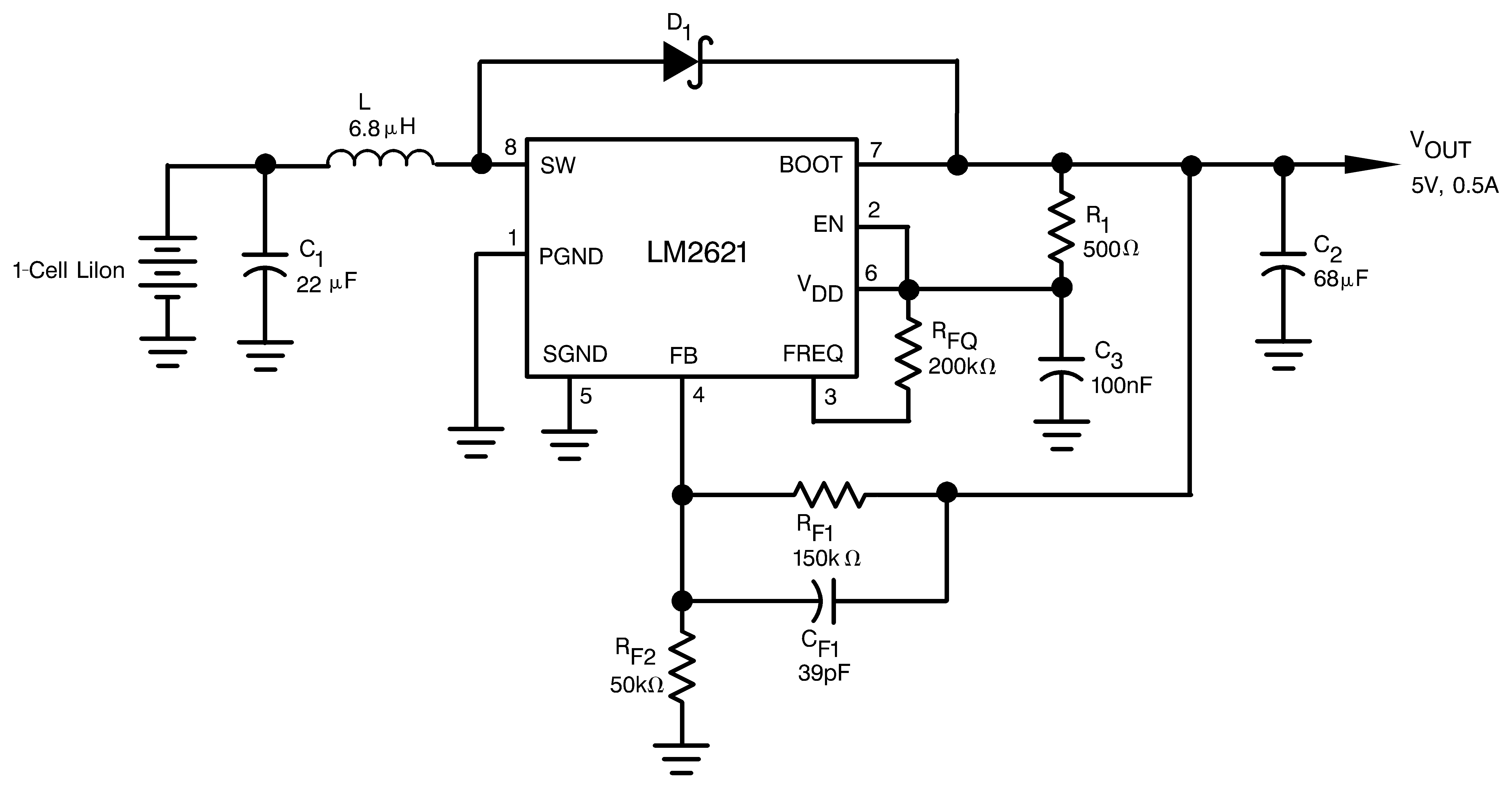
Typical Application Circuit
