SNVSA58C January 2015 – November 2017 LM26480-Q1
PRODUCTION DATA.
- 1 Features
- 2 Applications
- 3 Description
- 4 Revision History
- 5 Device Comparison Tables
- 6 Pin Configuration and Functions
-
7 Specifications
- 7.1 Absolute Maximum Ratings
- 7.2 ESD Ratings
- 7.3 Recommended Operating Conditions: Bucks
- 7.4 Thermal Information
- 7.5 General Electrical Characteristics
- 7.6 Low Dropout Regulators, LDO1 and LDO2
- 7.7 Buck Converters SW1, SW2
- 7.8 I/O Electrical Characteristics
- 7.9 Power-On Reset Threshold/Function (POR)
- 7.10 Typical Characteristics — LDO
- 7.11 Typical Characteristics — Buck 2.8 V to 5.5 V
- 7.12 Typical Characteristics — Bucks 1 and 2
- 7.13 Typical Characteristics — Buck 3.6 V
-
8 Detailed Description
- 8.1 Overview
- 8.2 Functional Block Diagram
- 8.3
Feature Description
- 8.3.1
DC-DC Converters
- 8.3.1.1 Linear Low Dropout Regulators (LDOs)
- 8.3.1.2
SW1, SW2: Synchronous Step-Down Magnetic DC-DC Converters
- 8.3.1.2.1 Functional Description
- 8.3.1.2.2 Circuit Operation Description
- 8.3.1.2.3 PWM Operation
- 8.3.1.2.4 Internal Synchronous Rectification
- 8.3.1.2.5 Current Limiting
- 8.3.1.2.6 PFM Operation
- 8.3.1.2.7 SW1, SW2 Control
- 8.3.1.2.8 Shutdown Mode
- 8.3.1.2.9 Soft Start
- 8.3.1.2.10 Low Dropout Operation
- 8.3.1.2.11 Flexible Power-On Reset (Power Good with Delay)
- 8.3.1.2.12 Undervoltage Lockout
- 8.3.1
DC-DC Converters
- 8.4 Device Functional Modes
-
9 Application and Implementation
- 9.1 Application Information
- 9.2
Typical Application
- 9.2.1 Design Requirements
- 9.2.2 Detailed Design Procedure
- 9.2.3 Application Curves
- 10Power Supply Recommendations
- 11Layout
- 12Device and Documentation Support
- 13Mechanical, Packaging, and Orderable Information
Package Options
Mechanical Data (Package|Pins)
- RTW|24
Thermal pad, mechanical data (Package|Pins)
- RTW|24
Orderable Information
1 Features
- Qualified for Automotive Applications
- AEC Q100-Qualified With the Following Results
- Device Temperature Grade 1: –40°C to +125°C Ambient Operating Temperature Range
- Input Voltage: 2.8 V to 5.5 V
- Compatible with Advanced Applications Processors and FPGAs
- Two LDOs for Powering Internal Processor Functions and I/Os
- Precision Internal Reference
- Thermal Overload Protection
- Current Overload Protection
- External Power-On-Reset Function for Buck1 and Buck2
- Undervoltage Lockout Detector to Monitor Input Supply Voltage
-
Step-Down DC-DC Converters (Buck)
- 1.5-A Output Current
- VOUT from:
- Buck1 : 0.8 V to 2 V at 1.5 A
- Buck2 : 1 V to 3.3 V at 1.5 A
- Up to 96% efficiency
- ±3% FB Voltage Accuracy
- 2-MHz PWM Switching Frequency
- PWM-to-PFM Automatic Mode Change Under Low Loads
- Automatic Soft Start
-
Linear Regulators (LDO)
- VOUT of 1 V to 3.5 V
- ±3% FB Voltage Accuracy
- 300-mA Output Current
- 25-mV (Typical) Dropout
2 Applications
- Core Digital Power
- Applications Processors
- Peripheral I/O Power
3 Description
The LM26480-Q1 is an automotive-qualified multi-functional power management unit (PMU), optimized for low-power digital applications. This device integrates two highly efficient 1.5-A step-down DC-DC converters and two 300-mA linear regulators. The DC-DC buck converters provide typical efficiencies of 96%, allowing for minimal power consumption. Features include soft start, undervoltage lockout, current overload protection, thermal overload protection, and an internal power-on-reset (POR) circuit, which monitors the output voltage levels on bucks 1 and 2.
Device Information(1)
| PART NUMBER | PACKAGE | BODY SIZE (NOM) |
|---|---|---|
| LM26480-Q1 | WQFN (24) | 4.00 mm × 4.00 mm |
- For all available packages, see the orderable addendum at the end of the data sheet.
space
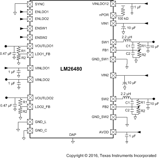
Simplified Schematic

4 Revision History
Changes from B Revision (December 2016) to C Revision
- Deleted the maximum lead temperature (soldering) from the Absolute Maximum Ratings tableGo
- Changed the PBUCK1 and PBUCK2 equations in the Junction Temperature sectionGo
- Changed the Electrostatic Discharge Caution statement Go
Changes from A Revision (June 2016) to B Revision
- Changed data sheet title; add content to Description section Go
Changes from * Revision (January 2016) to A Revision