SNOS977F May 2001 – May 2016 LM397
PRODUCTION DATA.
- 1 Features
- 2 Applications
- 3 Description
- 4 Revision History
- 5 Pin Configuration and Functions
- 6 Specifications
- 7 Detailed Description
- 8 Application and Implementation
- 9 Power Supply Recommendations
- 10Layout
- 11Device and Documentation Support
- 12Mechanical, Packaging, and Orderable Information
Package Options
Mechanical Data (Package|Pins)
- DBV|5
Thermal pad, mechanical data (Package|Pins)
Orderable Information
1 Features
- TA = 25°C. Typical Values Unless Otherwise Specified.
- 5-Pin SOT-23 Package
- Industrial Operating Range −40°C to +85°C
- Single or Dual Power Supplies
- Wide Supply Voltage Range 5 V to 30 V
- Low Supply Current 300 µA
- Low Input Bias Current 7 nA
- Low Input Offset Current ±1 nA
- Low Input Offset Voltage ±2 mV
- Response Time 440 ns (50-mV Overdrive)
- Input Common-Mode Voltage 0 to VS – 1.5 V
2 Applications
- A/D Converters
- Pulse, Square-Wave Generators
- Peak Detector
- Industrial Applications
3 Description
The LM397 device is a single voltage comparator with an input common mode that includes ground. The LM397 is designed to operate from a single 5-V to 30-V power supply or a split power supply. Its low supply current is virtually independent of the magnitude of the supply voltage.
The LM397 features an open-collector output stage. This allows the connection of an external resistor at the output. The output can directly interface with TTL, CMOS and other logic levels, by tying the resistor to different voltage levels (level translator).
The LM397 is available in the space-saving 5-Pin SOT-23 package and is pin-compatible to TI’s TL331, a single differential comparator.
Device Information(1)
| PART NUMBER | PACKAGE | BODY SIZE (NOM) |
|---|---|---|
| LM397 | SOT-23 (5) | 2.90 mm × 1.60 mm |
- For all available packages, see the orderable addendum at the end of the data sheet.
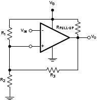
Typical Circuit
