SNVSA83C April 2015 – October 2017 LM43602-Q1
PRODUCTION DATA.
- 1 Features
- 2 Applications
- 3 Description
- 4 Revision History
- 5 Pin Configuration and Functions
- 6 Specifications
-
7 Detailed Description
- 7.1 Overview
- 7.2 Functional Block Diagram
- 7.3
Feature Description
- 7.3.1 Fixed Frequency Peak Current Mode Controlled Step-Down Regulator
- 7.3.2 Light Load Operation
- 7.3.3 Adjustable Output Voltage
- 7.3.4 Enable (EN)
- 7.3.5 VCC, UVLO, and BIAS
- 7.3.6 Soft Start and Voltage Tracking (SS/TRK)
- 7.3.7 Switching Frequency (RT) and Synchronization (SYNC)
- 7.3.8 Minimum ON Time, Minimum OFF Time and Frequency Foldback at Dropout Conditions
- 7.3.9 Internal Compensation and CFF
- 7.3.10 Bootstrap Voltage (BOOT)
- 7.3.11 Power Good (PGOOD)
- 7.3.12 Overcurrent and Short Circuit Protection
- 7.3.13 Thermal Shutdown
- 7.4 Device Functional Modes
-
8 Applications and Implementation
- 8.1 Application Information
- 8.2
Typical Applications
- 8.2.1 Design Requirements
- 8.2.2
Detailed Design Procedure
- 8.2.2.1 Custom Design With WEBENCH® Tools
- 8.2.2.2 Output Voltage Set-Point
- 8.2.2.3 Switching Frequency
- 8.2.2.4 Input Capacitors
- 8.2.2.5 Inductor Selection
- 8.2.2.6 Output Capacitor Selection
- 8.2.2.7 Feed-Forward Capacitor
- 8.2.2.8 Bootstrap Capacitors
- 8.2.2.9 VCC Capacitor
- 8.2.2.10 BIAS Capacitors
- 8.2.2.11 Soft-Start Capacitors
- 8.2.2.12 Undervoltage Lockout Setpoint
- 8.2.2.13 PGOOD
- 8.2.3 Application Performance Curves
- 9 Power Supply Recommendations
- 10Layout
- 11Device and Documentation Support
- 12Mechanical, Packaging, and Orderable Information
Package Options
Mechanical Data (Package|Pins)
- PWP|16
Thermal pad, mechanical data (Package|Pins)
Orderable Information
1 Features
- Qualified for Automotive Applications
- AEC-Q100 Qualified With the Following Results:
- Device Temperature Grade 2: –40°C to +125°C Ambient Operating Temperature
- 27-µA Quiescent Current in Regulation
- High Efficiency at Light Load (DCM and PFM)
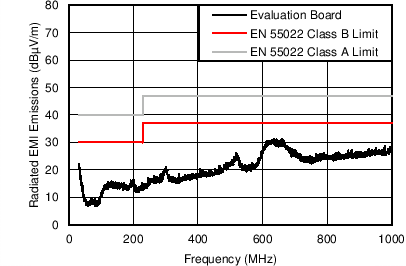
- Meets EN55022/CISPR 22 EMI Standards
- Integrated Synchronous Rectification
- Adjustable Frequency Range: 200 kHz to 2.2 MHz (500 kHz default)
- Frequency Synchronization to External Clock
- Internal Compensation
- Stable with Almost Any Combination of Ceramic, Polymer, Tantalum, and Aluminum Capacitors
- Power-Good Flag
- Soft Start into a Pre-Biased Load
- Internal Soft Start: 4.1 ms
- Extendable Soft-Start Time by External Capacitor
- Output Voltage Tracking Capability
- Precision Enable to Program System UVLO
- Output Short-Circuit Protection with Hiccup Mode
- Overtemperature Thermal Shutdown Protection
- Create a Custom Design Using the LM43602-Q1 With the WEBENCH® Power Designer
2 Applications
3 Description
The LM43602-Q1 regulator is an easy-to-use synchronous step-down DC-DC converter capable of driving up to 2 A of load current from an input voltage ranging from 3.5 V to 36 V (42 V abs maximum). The LM43602-Q1 provides exceptional efficiency, output accuracy and dropout voltage in a very small solution size. An extended family is available in 0.5-A , 1-A, and 3-A load current options in pin-to-pin compatible packages. Peak current mode control is employed to achieve simple control loop compensation and cycle-by-cycle current limiting. Optional features such as programmable switching frequency, synchronization, power-good flag, precision enable, internal soft-start, extendable soft-start, and tracking provide a flexible and easy to use platform for a wide range of applications. Discontinuous conduction and automatic frequency modulation at light loads improve light load efficiency. The family requires few external components and pin arrangement allows simple, optimum PCB layout. Protection features include thermal shutdown, VCC undervoltage lockout, cycle-by-cycle current limit, and output short-circuit protection. The LM43602-Q1 device is available in the HTSSOP (PWP) 16-pin leaded package (6.6 mm × 5.1 mm × 1.2 mm).The LM43602A-Q1 version is optimized for PFM operation and recommended for new designs. The device is pin-to-pin compatible with LM4360x and LM4600x family.
Device Information
| PART NUMBER | PACKAGE | BODY SIZE |
|---|---|---|
| LM43602-Q1 | HTSSOP (16) | 6.60 mm × 5.10 mm |
| LM43602A-Q1 | HTSSOP (16) | 6.60 mm × 5.10 mm |
space
space
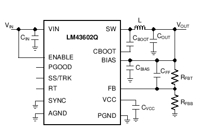
Simplified Schematic

Radiated Emission Graph
12VIN to 3.3 VOUT FS = 500 kHz IOUT = 2 A
