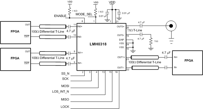
The LMH0318 is a 3 Gbps HD/SD SDI Reclocker with Integrated Cable Driver designed to drive serial video data compatible to SMPTE-SDI and DVB-ASI standards. The clock and data recovery circuit eliminates accumulated jitter and detects the incoming data rate without requiring an external reference clock. The integrated driver with 75 ohm and 50 ohm outputs enables multiple media options such as coax and FR4 PCB.
PART NUMBER | PACKAGE | BODY SIZE (NOM) |
---|---|---|
LMH0318 | WQFN (24) | 4 mm × 4 mm |
DATE | REVISION | NOTES |
---|---|---|
September 2015 | * | Initial release. |
The integrated 2-to-1 MUX on the input of the LMH0318 enables selection between two video sources, while the programmable equalizer compensates for the PC board loss to extend signal reach. With a wide range clock-and-data recovery (CDR) circuit, the on-chip reclocker automatically detects and locks to serial data from 270 Mbps to 2.97 Gbps without the need for an external reference clock and loop filter component, thereby simplifying board design and lowering system cost. The reclocked serial data can be routed to either the 75 Ω or 50 Ω transmitter output, or both simultaneously (1-to-2 fanout mode). The output voltage swing is compatible to ST 424, 344, 292, and 259 standards.
A non-disruptive eye monitor allows for real-time measurement of serial data to simplify system startup or field tuning. The LMH0318 is pin compatible with the LMH1218, 12 Gbps Cable Driver with Integrated Reclocker.
PIN | I/O | DESCRIPTION | |
---|---|---|---|
NAME | NO. | ||
CONTROL/INDICATOR I/O | |||
MODE_SEL | 1 | Input, 4-Level | Determines Device Configuration: SPI or SMBus 1 kΩ to VDD:
|
SS_N | 2 | Input, 2-Level | SPI Slave Select. . This pin has internal pull up |
SCK | 3 | Input, 2.5V LVCMOS, 2-Level | SPI serial clock input |
MOSI | 4 | Input, 2-Level | SPI Master Output / Slave Input. LMH0318 SPI data receive |
RESERVED | 5,14,17, 18 |
No Connect | |
ENABLE | 6 | Input, 4-Level | Powers down device when pulled low 1 kΩ to VDD:
Float(Default):
20 kΩ to GND:
1 kΩ to GND:
|
LOS_INT_N | 13 | Output, LVCMOS Open Drain, 2-Level |
Programmable Interrupt caused by change in LOS, violation of internal eye monitor threshold, or change in lock. External 4.7-kΩ pull-up resistor is required. This pin is 3.3 V LVCMOS tolerant. |
MISO | 15 | Output, 2.5 V LVCMOS, 2-Level | SPI Master Input / Slave Output. LMH0318 SPI data transmit |
LOCK | 16 | Output, 2.5V LVCMOS, 2-Level | Indicates CDR lock detect status High:
Low:
|
HIGH SPEED DIFFERENTIAL I/O | |||
IN0+ | 11 | Input, Analog | Inverting and non-inverting differential inputs. An on-chip 100 Ω terminating resistor connects IN0+ to IN0-. Inputs require 4.7 µF AC coupling capacitors. |
IN0- | 12 | Input, Analog | |
IN1+ | 8 | Input, Analog | Inverting and non-inverting differential inputs. An on-chip 100 Ω terminating resistor connects IN1+ to IN1-. Inputs require 4.7 µF AC coupling capacitors. |
IN1- | 9 | Input, Analog | |
OUT0+ | 20 | Output, 75 Ω CML Compatible | Inverting and non-inverting 75 Ω outputs. An on-chip 75 Ω terminating resistor connects OUT0+ and OUT0- to VDD. Outputs require 4.7 µF AC coupling capacitors |
OUT0- | 19 | Output, 75 Ω CML Compatible | |
OUT1+ | 23 | Output, Analog | Inverting and non-inverting differential outputs. An on-chip 100 Ω terminating resistor connects OUT1+ to OUT1-. Outputs require 4.7 µF AC coupling capacitors |
OUT1- | 22 | Output, Analog | |
POWER | |||
VDD | 7, 21 | 2.5 V Supply | 2.5 V ± 5% |
VSS | 10, 24 | Ground | Connect directly to ground (GND) |
DAP | Ground | Exposed DAP, connect to GND using at least 5 vias (see Figure 23 ) |
PIN | I/O | DESCRIPTION | |
---|---|---|---|
NAME | NO. | ||
MODE_SEL | 1 | Input, 4-Level | Determines Device Configuration: SPI or SMBus 1 kΩ to GND: SMBUS mode. See Initialization Set Up |
ADDR0 | 2 | Input, 4-Level | 4-level strap pins used to set the SMBus address of the device. The pin state is read on power-up. The multi-level nature of these pins allows for 16 unique device addresses. Note SMBus section for further details. The four strap options include: 1 kΩ to VDD:
Float(Default): Represents logic state 10'b 7-bits SMBus address = 0x17 20 kΩ to GND:
1 kΩ to GND:
|
ADDR1 | 15 | ||
SCL | 3 | Input, 2-Level | SMBus clock input / open drain. External 2-kΩ to 5-kΩ pull-up resistor is required as per SMBus interface standard. This pin is 3.3 V LVCMOS tolerant. |
SDA | 4 | I/O, Open Drain, 2-Level | SMBus data input / open drain. External 2-kΩ to 5-kΩ pull-up resistor is required as per SMBus interface standard. This pin is 3.3 V LVCMOS tolerant. |
RESERVED | 5,14,17, 18 |
No Connect | |
ENABLE | 6 | Input, 4-Level | Powers down device when pulled low 1 kΩ to VDD:
Float(Default): Reserved 20 kΩ to GND:
1 kΩ to GND:
|
LOS_INT_N | 13 | Output, LVCMOS Open Drain, 2-Level |
Programmable Interrupt caused by change in LOS, violation of internal eye monitor threshold, change in lock. External 4.7-kΩ pull-up resistor is required. This pin is 3.3 V LVCMOS tolerant. |
LOCK | 16 | Output, 2.5 V LVCMOS, 2-Level | Indicates CDR lock Status High:
Low:
|
HIGH SPEED DIFFERENTIAL I/O | |||
IN0+ | 11 | Input, Analog | Inverting and non-inverting differential inputs. An on-chip 100 Ω terminating resistor connects IN0+ to IN0-. Inputs require 4.7 µF AC coupling capacitors. |
IN0- | 12 | Input, Analog | |
IN1+ | 8 | Input, Analog | Inverting and non-inverting differential inputs. An on-chip 100 Ω terminating resistor connects IN0+ to IN0-. Inputs require 4.7 µF AC coupling capacitors. |
IN1- | 9 | Input, Analog | |
OUT0+ | 20 | Output, 75 Ω CML Compatible | Inverting and non-inverting 75 Ω outputs. An on-chip 75 Ω terminating resistor connects OUT0+ and OUT0- to VDD. Outputs require 4.7 µF AC coupling capacitors |
OUT0- | 19 | Output, 75 Ω CML Compatible | |
OUT1+ | 23 | Output, Analog | Inverting and non-inverting differential outputs. An on-chip 100 Ω terminating resistor connects OUT1+ to OUT1-. Outputs require 4.7 µF AC coupling capacitors |
OUT1- | 22 | Output, Analog | |
VDD | 7, 21 | 2.5 V Supply | 2.5V ± 5% |
VSS | 10, 24 | Ground | Connect directly to ground (GND) |
DAP | Ground | Exposed DAP, connect to GND using at least 5 vias (see Figure 23 ) |