SBOS730A April 2015 – May 2015 LMH6401
PRODUCTION DATA.
- 1 Features
- 2 Applications
- 3 Description
- 4 Revision History
- 5 Device Options
- 6 Pin Configuration and Functions
- 7 Specifications
- 8 Parameter Measurement Information
-
9 Detailed Description
- 9.1 Overview
- 9.2 Functional Block Diagram
- 9.3 Feature Description
- 9.4 Device Functional Modes
- 9.5 Programming
- 9.6
Register Maps
- 9.6.1 Revision ID (address = 0h, Read-Only) [default = 03h]
- 9.6.2 Product ID (address = 1h, Read-Only) [default = 00h]
- 9.6.3 Gain Control (address = 2h) [default = 20h]
- 9.6.4 Reserved (address = 3h) [default = 8Ch]
- 9.6.5 Thermal Feedback Gain Control (address = 4h) [default = 27h]
- 9.6.6 Thermal Feedback Frequency Control (address = 5h) [default = 45h]
- 10Application and Implementation
- 11Power-Supply Recommendations
- 12Layout
- 13Device and Documentation Support
- 14Mechanical, Packaging, and Orderable Information
Package Options
Mechanical Data (Package|Pins)
- RMZ|16
Thermal pad, mechanical data (Package|Pins)
Orderable Information
1 Features
- 3-dB Bandwidth: 4.5 GHz at 26-dB Gain
- Gain Range: –6 dB to 26 dB in 1-dB Steps
- Differential Input Impedance: 100 Ω
- Differential Output with Common-Mode Control
- Distortion at Max Gain (VO = 2 VPPD, RL = 200 Ω):
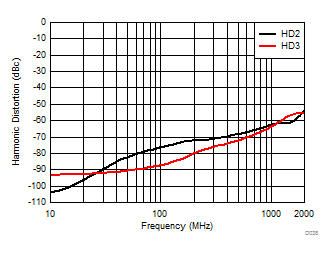
- 200 MHz: HD2 at –73 dBc, HD3 at –80 dBc
- 500 MHz: HD2 at –68 dBc, HD3 at –72 dBc
- 1 GHz: HD2 at –63 dBc, HD3 at –63 dBc
- 2 GHz: HD2 at –58 dBc, HD3 at –54 dBc
- Output IP3:
- 43 dBm at 200 MHz
- 33 dBm at 1 GHz
- 27 dBm at 2 GHz
- Output IP2:
- 67 dBm at 200 MHz
- 60 dBm at 1 GHz
- 52 dBm at 2 GHz
- 8-dB Noise Figure at 1 GHz, RS = 100 Ω
- 82-ps Rise, Fall Time Pulse Response
- Supply Operation: 5.0 V at 69 mA
- Supports Single- and (±) Split-Supply Operation:
- DC- and AC-Coupled Applications
- Fabricated on an Advanced Complementary BiCMOS Process
- 3-mm × 3-mm UQFN-16 Package
2 Applications
- Test and Measurement
- Ultra-Wideband ADC Drivers
- Communications Receivers
- RF Sampling Subsystems
- SAW Filter Buffers and Drivers
- Defense and Radar
3 Description
The LMH6401 is a wideband, digitally-controlled, variable-gain amplifier (DVGA) designed for dc to radio frequency (RF), intermediate frequency (IF), and high-speed time-domain applications. The device is an ideal analog-to-digital converter (ADC) driver for dc- or ac-coupled applications that require an automatic gain control (AGC).
Noise and distortion performance is optimized to drive ultra-wideband ADCs. The amplifier has an 8-dB noise figure at maximum gain and a –63-dBc harmonic distortion at 1 GHz for full-scale signal levels. The device supports both single- and split-supply operation for driving an ADC. A common-mode reference input pin is provided to align the amplifier output common-mode with the ADC input requirements.
Gain control is performed via an SPI™ interface, allowing a 32-dB gain range from –6 dB to 26 dB in 1-dB steps. A power-down feature is also available through the external PD pin or SPI control.
This level of performance is achieved at a low power level of 345 mW. The operating ambient temperature range is –40°C to 85°C.
Device Information(1)
| PART NUMBER | PACKAGE | BODY SIZE (NOM) |
|---|---|---|
| LMH6401 | UQFN (16) | 3.00 mm × 3.00 mm |
- For all available packages, see the orderable addendum at the end of the data sheet.
Harmonic Distortion vs Frequency (VO = 2 VPPD)

IF Sampling Receiver Application
