SNOSAI9I September 2005 – November 2015 LMP7701 , LMP7702 , LMP7704
PRODUCTION DATA.
- 1 Features
- 2 Applications
- 3 Description
- 4 Revision History
- 5 Description (continued)
- 6 Pin Configuration and Functions
- 7 Specifications
- 8 Detailed Description
- 9 Application and Implementation
- 10Power Supply Recommendations
- 11Layout
- 12Device and Documentation Support
- 13Mechanical, Packaging, and Orderable Information
Package Options
Mechanical Data (Package|Pins)
Thermal pad, mechanical data (Package|Pins)
Orderable Information
1 Features
- Unless Otherwise Noted,
Typical Values at VS = 5 V - Input Offset Voltage (LMP7701): ±200-µV (Maximum)
- Input Offset Voltage (LMP7702/LMP7704): ±220-µV (Maximum)
- Input Bias Current: ±200 fA
- Input Bias Current: ±200 fA
- Input Voltage Noise: 9 nV/√Hz
- CMRR: 130 dB
- Open-Loop Gain: 130 dB
- Temperature Range: −40°C to 125°C
- Unity-Gain Bandwidth: 2.5 MHz
- Supply Current (LMP7701): 715 µA
- Supply Current (LMP7702): 1.5 mA
- Supply Current (LMP7704): 2.9 mA
- Supply Voltage Range: 2.7 V to 12 V
- Rail-to-Rail Input and Output
2 Applications
- High Impedance Sensor Interface
- Battery-Powered Instrumentation
- High Gain Amplifiers
- DAC Buffer
- Instrumentation Amplifier
- Active Filters
3 Description
The LMP770x are single, dual, and quad low-offset voltage, rail-to-rail input and output precision amplifiers, each with a CMOS input stage and a wide supply voltage range. The LMP770x are part of the LMP™ precision amplifier family and are ideal for sensor interface and other instrumentation applications.
The specified low-offset voltage of less than ±200 µV, along with the specified low input bias current of less than ±1 pA, make the LMP7701 ideal for precision applications. The LMP770x are built using VIP50 technology, which allows the combination of a CMOS input stage and a 12-V common-mode and supply voltage range. This makes the LMP770x ideal for applications where conventional CMOS parts cannot operate under the desired voltage conditions.
Device Information(1)
| PART NUMBER | PACKAGE | BODY SIZE (NOM) |
|---|---|---|
| LMP7701 | SOT-23 (5) | 1.60 mm × 2.90 mm |
| SOIC (8) | 3.91 mm × 4.90 mm | |
| LMP7702 | VSSOP (8) | 3.00 mm × 3.00 mm |
| SOIC (8) | 3.91 mm × 4.90 mm | |
| LMP7704 | TSSOP (14) | 4.40 mm × 5.00 mm |
| SOIC (14) | 3.91 mm × 8.65 mm |
- For all available packages, see the orderable addendum at the end of the data sheet.
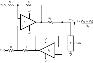
Typical Application Schematic
