SNOSAW3D September 2007 – August 2016 LMV641
PRODUCTION DATA.
- 1 Features
- 2 Applications
- 3 Description
- 4 Revision History
- 5 Pin Configuration and Functions
- 6 Specifications
- 7 Detailed Description
- 8 Application and Implementation
- 9 Power Supply Recommendations
- 10Layout
- 11Device and Documentation Support
- 12Mechanical, Packaging, and Orderable Information
Package Options
Mechanical Data (Package|Pins)
Thermal pad, mechanical data (Package|Pins)
Orderable Information
1 Features
- Specified for 2.7-V, and ±5-V Performance
- Low Power Supply Current: 138 µA
- High Unity Gain Bandwidth: 10 MHz
- Max Input Offset Voltage: 500 µV
- CMRR: 120 dB
- PSRR: 105 dB
- Input Referred Voltage Noise: 14 nV/√Hz
- 1/f Corner Frequency: 4 Hz
- Output Swing With 2-kΩ Load 40 mV from Rail
- Total Harmonic Distortion: 0.002% at 1 kHz, 2 kΩ
- Temperature Range −40°C to 125°C
3 Description
The LMV641 is a low-power, wide-bandwidth operational amplifier with an extended power supply voltage range of 2.7 V to 12 V.
The device features 10 MHz of gain bandwidth product with unity gain stability on a typical supply current of 138 µA. Other key specifications are a PSRR of 105 dB, CMRR of 120 dB, VOS of 500 µV, input referred voltage noise of 14 nV/√Hz, and a THD of 0.002%. This amplifier has a rail-to-rail output stage and a common mode input voltage, which includes the negative supply.
The LMV641 device operates over a temperature range of −40°C to +125°C and is offered in the board-space-saving 5-Pin SC70, SOT-23, and 8-Pin SOIC packages.
Device Information(1)
| PART NUMBER | PACKAGE | BODY SIZE (NOM) |
|---|---|---|
| LMV641 | SOIC (8) | 4.90 mm × 3.91 mm |
| SOT-23 (5) | 2.90 mm × 1.60 mm | |
| SC70 (5) | 2.00 mm × 1.25 mm |
- For all available packages, see the orderable addendum at the end of the data sheet.
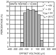
Offset Voltage Distribution

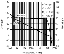
Open Loop Gain and Phase vs Frequency
