SNAS187D February   2003  – January 2016 LMX2430 , LMX2433 , LMX2434

PRODUCTION DATA.  

  1. Features
  2. Applications
  3. Description
  4. Revision History
  5. Description continued
  6. Pin Configuration and Functions
  7. Specifications
    1. 7.1 Absolute Maximum Ratings
    2. 7.2 Recommended Operating Conditions
    3. 7.3 Thermal Information
    4. 7.4 Electrical Characteristics
    5. 7.5 Timing Requirements
    6. 7.6 Typical Characteristics
      1. 7.6.1 Sensitivity
      2. 7.6.2 Charge Pump
      3. 7.6.3 Input Impedance
  8. Parameter Measurement Information
    1. 8.1 Bench Test Setups
      1. 8.1.1 LMX243x Charge-Pump Test Setup
      2. 8.1.2 Charge-Pump Current Specification Definitions
        1. 8.1.2.1 Charge-Pump Output Current Variation vs Charge-Pump Output Voltage
        2. 8.1.2.2 Charge-Pump Sink Current vs Charge-Pump Output Source Current Mismatch
        3. 8.1.2.3 Charge-Pump Output Current Variation vs Temperature
      3. 8.1.3 LMX243x FinRF Sensitivity Test Setup
      4. 8.1.4 LMX243x OSCin Sensitivity Test Setup
      5. 8.1.5 LMX243x FinRF Input Impedance Test Setup
  9. Detailed Description
    1. 9.1 Overview
    2. 9.2 Functional Block Diagram
    3. 9.3 Feature Description
      1. 9.3.1  Reference Oscillator Input
      2. 9.3.2  Reference Dividers (R Counters)
      3. 9.3.3  Prescalers
      4. 9.3.4  Programmable Feedback Dividers (N Counters)
      5. 9.3.5  Phase / Frequency Detectors
        1. 9.3.5.1 Phase Comparator and Internal Charge-Pump Characteristics
      6. 9.3.6  Charge Pumps
      7. 9.3.7  Microwire Serial Interface
      8. 9.3.8  Multi-Function Outputs
        1. 9.3.8.1 Push-Pull Analog Lock-Detect Output
        2. 9.3.8.2 Open-Drain Analog Lock-Detect Output
        3. 9.3.8.3 Digital Filtered Lock-Detect Output
        4. 9.3.8.4 Reference Divider and Feedback Divider Output
      9. 9.3.9  Fastlock Output
      10. 9.3.10 Counter Reset
    4. 9.4 Device Functional Modes
      1. 9.4.1 Power Control
        1. 9.4.1.1 Synchronous Power-Down Mode
        2. 9.4.1.2 Asynchronous Power-Down Mode
    5. 9.5 Programming
      1. 9.5.1 Microwire Interface
      2. 9.5.2 Control Register Location
    6. 9.6 Register Maps
      1. 9.6.1 Control Register Content Map
      2. 9.6.2 R0 Register
        1. 9.6.2.1 RF_R[14:0] - RF Synthesizer Programmable Reference Divider (R Counter) (R0[17:3])
        2. 9.6.2.2 RF_CPP - RF Synthesizer Phase Detector Polarity (R0[18])
        3. 9.6.2.3 RF_CPG - RF Synthesizer Charge-Pump Current Gain (R0[19])
        4. 9.6.2.4 RF_CPT - RF Synthesizer Charge-Pump Tri-State (R0[20])
        5. 9.6.2.5 RF_RST - RF Synthesizer Counter Reset (R0[21])
      3. 9.6.3 R1 Register
        1. 9.6.3.1 LMX243x RF Synthesizer Swallow Counter
          1. 9.6.3.1.1 RF_A[3:0] - LMX2430/33 RF Synthesizer Swallow Counter (A Counter) (R1[6:3])
          2. 9.6.3.1.2 RF_A[4:0] - LMX2434 RF Synthesizer Swallow Counter (A Counter) (R1[7:3])
        2. 9.6.3.2 LMX243x RF Synthesizer Programmable Binary Counter
          1. 9.6.3.2.1 RF_B[14:0] - LMX2430/33 RF Synthesizer Programmable Binary Counter (B Counter) (R1[21:7])
          2. 9.6.3.2.2 RF_B[13:0] - LMX2434 RF Synthesizer Programmable Binary Counter (B Counter) (R1[21:8])
        3. 9.6.3.3 LMX243x RF Synthesizer Prescaler Select
          1. 9.6.3.3.1 RF_P - LMX2430/33 RF Synthesizer Prescaler Select (R1[22])
          2. 9.6.3.3.2 RF_P - LMX2434 RF Synthesizer Prescaler Select (R1[22])
        4. 9.6.3.4 RF_PD - RF Synthesizer Power Down (R1[23])
      4. 9.6.4 R2 Register
        1. 9.6.4.1 RF_TOC[0:11] - RF Synthesizer Time-Out Counter (R2[14:3])
        2. 9.6.4.2 R3 Register
          1. 9.6.4.2.1 IF_R[14:0] - IF Synthesizer Programmable Reference Divider (R Counter) (R3[17:3])
          2. 9.6.4.2.2 IF_CPP - IF Synthesizer Phase Detector Polarity (R3[18])
          3. 9.6.4.2.3 IF_CPG - IF Synthesizer Charge-Pump Current Gain (R3[19])
          4. 9.6.4.2.4 IF_CPT - IF Synthesizer Charge-Pump Tri-State (R3[20])
          5. 9.6.4.2.5 IF_RST - IF Synthesizer Counter Reset (R3[21])
      5. 9.6.5 R4 Register
        1. 9.6.5.1 IF_A[3:0] - IF Synthesizer Swallow Counter (A Counter) (R4[6:3])
        2. 9.6.5.2 IF_B[13:0] - IF Synthesizer Programmable Binary Counter (B Counter) (R4[20:7])
          1. 9.6.5.2.1 IF_P - IF Synthesizer Prescaler Select (R4[22])
        3. 9.6.5.3 IF_PD - IF Synthesizer Power Down (R4[23])
      6. 9.6.6 R5 Register
        1. 9.6.6.1 IF_TOC[0:11] - IF Synthesizer Time-Out Counter (R5[14:3])
      7. 9.6.7 MUX[3:0] - Multifunction Output Select (R3[23:22]:R0[23:22])
  10. 10Application and Implementation
    1. 10.1 Application Information
    2. 10.2 Typical Application
      1. 10.2.1 Design Requirements
      2. 10.2.2 Detailed Design Procedure
      3. 10.2.3 Application Curves
  11. 11Power Supply Recommendations
  12. 12Layout
    1. 12.1 Layout Guidelines
    2. 12.2 Layout Example
  13. 13Device and Documentation Support
    1. 13.1 Device Support
      1. 13.1.1 Device Nomenclature
        1. 13.1.1.1 List of Definitions
    2. 13.2 Related Links
    3. 13.3 Community Resources
    4. 13.4 Trademarks
    5. 13.5 Electrostatic Discharge Caution
    6. 13.6 Glossary
  14. 14Mechanical, Packaging, and Orderable Information

Package Options

Mechanical Data (Package|Pins)
Thermal pad, mechanical data (Package|Pins)
Orderable Information

1 Features

  • Low Current Consumption
    • LMX2430 (RF/IF): 2.8 mA/ 1.4 mA
    • LMX2433 (RF/IF): 3.2 mA/ 2 mA
    • LMX2434 (RF/IF): 4.6 mA/ 2.4 mA
  • 2.25-V to 2.75-V Operation
  • Synchronous/Asynchronous Power Down
  • Multiple PLL Options:
    • LMX2430 (RF/IF): 3 GHz /0.8 GHz
    • LMX2433 (RF/IF): 3.6 GHz /1.7 GHz
    • LMX2434 (RF/IF): 5 GHz /2.5 GHz
  • Programmable Charge-Pump Current Levels
    • RF and IF: 1 or 4 mA
  • Fastlock With Integrated Time-Out Counters
  • Digital Filtered Lock-Detect Output
  • Analog Lock Detect (Push-Pull / Open-Drain)
  • 1.8-V MICROWIRE Logic Interface

2 Applications

  • Mobile Handsets
  • Cordless Handsets
  • Wireless Data
  • Cable TV Tuners

3 Description

Using a proprietary digital-phase, locked-loop technique, the LMX243x devices generate very stable, low-noise control signals for RF and IF voltage controlled oscillators. Both the RF and IF synthesizers include a two-level programmable charge pump. Both the RF and IF PLLs have dedicated fastlock circuitry with integrated time-out counters which require only a single word write to power up or change frequencies.

Device Information(1)

PART NUMBER PACKAGE BODY SIZE (NOM)
LMX243x ULGA (20) 3.50 mm × 3.50 mm
TSSOP (20) 6.50 mm × 4.40 mm
  1. For all available packages, see the orderable addendum at the end of the data sheet.

Functional Block Diagram
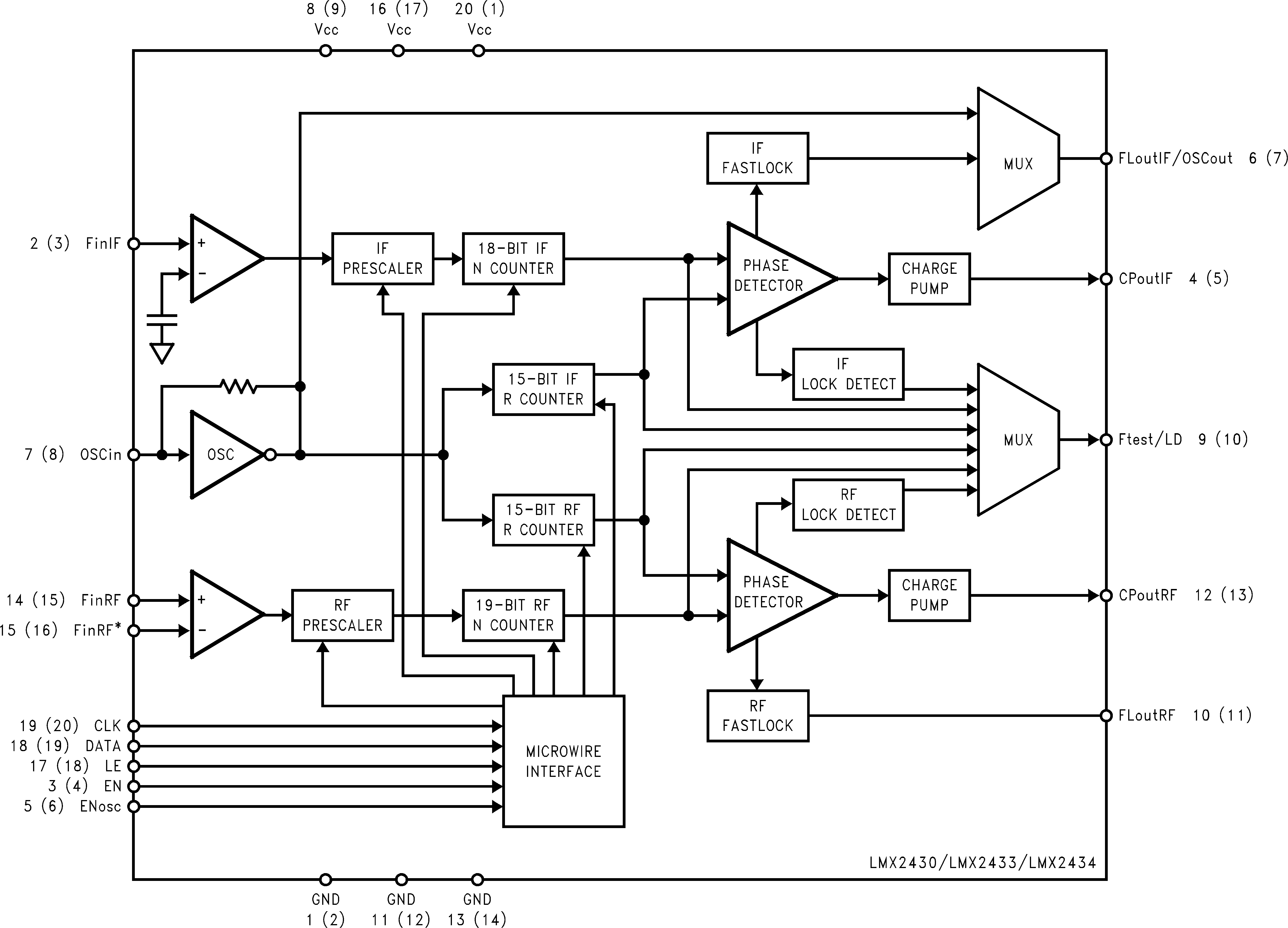
LMX2430 LMX2433 LMX2434 20053501.png

NOTE:

1 (2) refers to Pin 1 of the 20-Pin ULGA and Pin 2 of the 20-Pin TSSOP