SNOSB31J July 2009 – December 2014 LMX2541
PRODUCTION DATA.
- 1 Features
- 2 Applications
- 3 Description
- 4 Revision History
- 5 Device Comparison Table
- 6 Pin Configuration and Functions
- 7 Specifications
- 8 Parameter Measurement Information
-
9 Detailed Description
- 9.1 Overview
- 9.2 Functional Block Diagrams
- 9.3
Feature Description
- 9.3.1 PLL Reference Oscillator Input Pins
- 9.3.2 PLL R Divider
- 9.3.3 PLL Phase Detector and Charge Pump
- 9.3.4 PLL N Divider and Fractional Circuitry
- 9.3.5 Partially Integrated Loop Filter
- 9.3.6 Low Noise, Fully Integrated VCO
- 9.3.7 Programmable VCO Divider
- 9.3.8 Programmable RF Output Buffer
- 9.3.9 Powerdown Modes
- 9.3.10 Fastlock
- 9.3.11 Lock Detect
- 9.3.12 Current Consumption
- 9.3.13 Fractional Spurs
- 9.3.14 Impact of VCO_DIV on Fractional Spurs
- 9.3.15 PLL Phase Noise
- 9.3.16 Impact of Modulator Order, Dithering, and Larger Equivalent Fractions on Spurs and Phase Noise
- 9.3.17 Modulator Order
- 9.3.18 Programmable Output Power with On/Off
- 9.3.19 Loop Filter
- 9.3.20 Internal VCO Digital Calibration Time
- 9.4 Device Functional Modes
- 9.5 Programming
- 9.6
Register Maps
- 9.6.1
Register R7
- 9.6.1.1 Register R13
- 9.6.1.2 Register R12
- 9.6.1.3 Register R9
- 9.6.1.4 Register R8
- 9.6.1.5 Register R6
- 9.6.1.6 Register R5
- 9.6.1.7
Register R4
- 9.6.1.7.1 OSC_FREQ [7:0] -- OSCin Frequency for VCO Calibration Clocking
- 9.6.1.7.2 VCO_DIV[5:0] - VCO Divider
- 9.6.1.7.3 R3_LF[2:0] -- Value for Internal Loop Filter Resistor R3
- 9.6.1.7.4 R4_LF[2:0] -- Value for Internal Loop Filter Resistor R4
- 9.6.1.7.5 C3_LF[3:0] -- Value for C3 in the Internal Loop Filter
- 9.6.1.7.6 C4_LF[3:0] -- Value for C4 in the Internal Loop Filter
- 9.6.1.8
Register R3
- 9.6.1.8.1 MODE[1:0] -- Operational Mode
- 9.6.1.8.2 Powerdown -- Powerdown Bit
- 9.6.1.8.3 XO - Crystal Oscillator Mode Select
- 9.6.1.8.4 CPG[4:0] -- Charge Pump Current
- 9.6.1.8.5 MUX[3:0] -- Multiplexed Output for Ftest/LD Pin
- 9.6.1.8.6 CPP - Charge Pump Polarity
- 9.6.1.8.7 OSC2X-- OSCin Frequency Doubler
- 9.6.1.8.8 FDM - Extended Fractional Denominator Mode Enable
- 9.6.1.8.9 ORDER[2:0] -- Delta-Sigma Modulator Order
- 9.6.1.8.10 DITH[1:0] -- Dithering
- 9.6.1.8.11 CPT - Charge Pump TRI-STATE
- 9.6.1.8.12 DLOCK[2:0] - Controls for Digital Lock Detect
- 9.6.1.8.13 FSK - Frequency Shift Keying
- 9.6.1.9 Register R2
- 9.6.1.10 Registers R1 and R0
- 9.6.1
Register R7
-
10Application and Implementation
- 10.1
Application Information
- 10.1.1 Determining the Best Frequency Option of the LMX2541 to Use
- 10.1.2 RFout Output Power Test Setup
- 10.1.3 Phase Noise Measurement Test Setup
- 10.1.4 Input and Output Impedance Test Setup
- 10.1.5 ExtVCOin (NOT OSCin) Input Sensitivity Test Setup
- 10.1.6 OSCin Input Sensitivity Test Setup
- 10.1.7 Typical Connections
- 10.2 Typical Application
- 10.1
Application Information
- 11Power Supply Recommendations
- 12Layout
- 13Device and Documentation Support
- 14Mechanical, Packaging, and Orderable Information
Package Options
Refer to the PDF data sheet for device specific package drawings
Mechanical Data (Package|Pins)
- NJK|36
Thermal pad, mechanical data (Package|Pins)
Orderable Information
1 Features
- Multiple Frequency Options Available
(See Device Comparison Table) - Frequencies From 31.6 MHz to 4000 MHz
- Very Low RMS Noise and Spurs
- –225 dBc/Hz Normalized PLL Phase Noise
- Integrated RMS Noise (100 Hz to 20 MHz)
- 2 mRad (100 Hz to 20 MHz) at 2.1 GHz
- 3.5 mRad (100 Hz to 20 MHz) at 3.5 GHz
- Ultra Low-Noise Integrated VCO
- External VCO Option (Internal VCO Bypassed)
- VCO Frequency Divider 1 to 63 (All Values)
- Programmable Output Power
- Up to 104-MHz Phase Detector Frequency
- Integrated Low-Noise LDOs
- Programmable Charge Pump Output
- Partially Integrated Loop Filter
- Digital Frequency Shift Keying (FSK) Modulation Pin
- Integrated Reference Crystal Oscillator Circuit
- Hardware and Software Power Down
- FastLock Mode and VCO-Based Cycle Slip Reduction
- Analog and Digital Lock Detect
- 1.6-V Logic Compatibility
2 Applications
- Wireless Infrastructure (UMTS, LTE, WiMax)
- Broadband Wireless
- Wireless Meter Reading
- Test and Measurement
- FM Mobile Radio
3 Description
The LMX2541 device is an ultra low-noise frequency synthesizer which integrates a high-performance delta-sigma fractional N PLL, a VCO with fully integrated tank circuit, and an optional frequency divider. The PLL offers an unprecedented normalized noise floor of –225 dBc/Hz and can be operated with up to 104 MHz of phase-detector rate (comparison frequency) in both integer and fractional modes. The PLL can also be configured to work with an external VCO.
The LMX2541 integrates several low-noise, high-precision LDOs and output driver matching network to provide higher supply noise immunity and more consistent performance, while reducing the number of external components. When combined with a high-quality reference oscillator, the LMX2541 generates a very stable, ultra low-noise signal.
The LMX2541 is offered in a family of 6 devices with varying VCO frequency range from 1990 MHz up to 4 GHz. Using a flexible divider, the LMX2541 can generate frequencies as low as 31.6 MHz.
The LMX2541 is a monolithic integrated circuit, fabricated in a proprietary BiCMOS process. Device programming is facilitated using a three-wire MICROWIRE interface that can operate down to 1.6 volts. Supply voltage ranges from 3.15 V to 3.45 V. The LMX2541 is available in a 36-pin 6-mm × 6-mm × 0.8-mm WQFN package.
Device Information(1)
| PART NUMBER | PACKAGE | VCO FREQUENCY (MHz) |
|---|---|---|
| LMX2541SQ2060E | WQFN (36) | 1990 - 2240 |
| LMX2541SQ2380E | WQFN (36) | 2200 - 2530 |
| LMX2541SQ2690E | WQFN (36) | 2490 - 2865 |
| LMX2541SQ3030E | WQFN (36) | 2810 - 3230 |
| LMX2541SQ3320E | WQFN (36) | 3130 - 3600 |
| LMX2541SQ3740E | WQFN (36) | 3480 - 4000 |
- For all available packages, see the orderable addendum at the end of the data sheet.
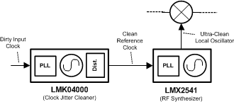
System Block Diagram
