SNVSA28 December 2014 LP8731-Q1
PRODUCTION DATA.
- 1 Features
- 2 Applications
- 3 Description
- 4 Revision History
- 5 Device Comparison Tables
- 6 Pin Configuration and Functions
-
7 Specifications
- 7.1 Absolute Maximum Ratings
- 7.2 ESD Ratings
- 7.3 Recommended Operating Conditions (Bucks)
- 7.4 Thermal Information
- 7.5 General Electrical Characteristics
- 7.6 Low Dropout Regulators, LDO1 And LDO2
- 7.7 Buck Converters SW1, SW2
- 7.8 I/O Electrical Characteristics
- 7.9 Power-On Reset Threshold/Function (POR)
- 7.10 I2C-Compatible Interface Timing
- 7.11 Typical Characteristics
-
8 Detailed Description
- 8.1 Overview
- 8.2 Functional Block Diagram
- 8.3
Features Description
- 8.3.1 Linear Low Dropout Regulators (LDOs)
- 8.3.2 No-Load Stability
- 8.3.3 LDO1 and LDO2 Control Registers
- 8.3.4
SW1, SW2: Synchronous Step-Down Magnetic DC-DC Converters
- 8.3.4.1 Functional Description
- 8.3.4.2 Circuit Operation
- 8.3.4.3 PWM Operation
- 8.3.4.4 Internal Synchronous Rectification
- 8.3.4.5 Current Limiting
- 8.3.4.6 SW1, SW2 Operation
- 8.3.4.7 SW1, SW2 Control Registers
- 8.3.4.8 Shutdown Mode
- 8.3.4.9 Soft Start
- 8.3.4.10 Low Dropout Operation
- 8.3.4.11 Flexible Power Sequencing of Multiple Power Supplies
- 8.3.4.12 Power-Up Sequencing Using the EN_T Function
- 8.3.5 Flexible Power-On Reset (for example, Power Good with Delay)
- 8.3.6 Undervoltage Lockout
- 8.4 Device Functional Modes
- 8.5 Programming
- 8.6
LP8731-Q1 Register Maps
- 8.6.1 Interrupt Status Register (ISRA) 0x02
- 8.6.2 System Control 1 Register (SCR1) 0x07
- 8.6.3 EN_DLY Preset Delay Sequence after EN_T Assertion
- 8.6.4 Buck and LDO Output Voltage Enable Register (BKLDOEN) - 0x10
- 8.6.5 Buck and LDO Status Register (BKLDOSR) - 0x11
- 8.6.6 BUCK Voltage Change Control Register 1 (VCCR) - 0x20
- 8.6.7 BUCK1 Target Voltage 1 Register (B1TV1) - 0x23
- 8.6.8 BUCK1 Target Voltage 2 Register (B1TV2) - 0x24
- 8.6.9 BUCK1 Ramp Control Register (B1RC) - 0x25
- 8.6.10 BUCK2 Target 1 Register (B2TV1) - 0x29
- 8.6.11 BUCK2 Target 2 Register (B2TV2) - 0x2A
- 8.6.12 BUCK2 Ramp Control Register (B2RC) - 0x2B
- 8.6.13 BUCK Function Register (BFCR) - 0x38
- 8.6.14 Spread Spectrum Function
- 8.6.15 LDO1 Control Register (LDO1VCR) - 0x39
- 8.6.16 LDO2 Control Register (LDO2VCR) - 0x3A
- 9 Application and Implementation
- 10Power Supply Recommendations
- 11Layout
- 12Device and Documentation Support
- 13Mechanical, Packaging, and Orderable Information
Package Options
Mechanical Data (Package|Pins)
- YZR|25
Thermal pad, mechanical data (Package|Pins)
Orderable Information
1 Features
- Two LDOs for Powering Internal Processor Functions and I/Os
- High-Speed Serial Interface for Independent Control of Device Functions and Settings
- Precision Internal Reference
- Thermal Overload Protection
- Current Overload Protection
- Software Programmable Regulators
- External Power-On-Reset Function for Buck1 and Buck2 (Power Good with Delay Function)
- Undervoltage Lockout (UVLO)
- LP8731-Q1 is an Automotive-Grade Product: AECQ-100 Grade-1 Qualified
-
Step-Down DC/DC Converter (2xBuck)
- Programmable VOUT from:
- Buck1 : 0.8875 V – 1.675 V at 1.2 A
- Buck2 : 0.8875 V – 1.675 V at 1.2 A
- Up to 96% Efficiency
- PWM Switching Frequency of 2.1 MHz
- ±2% Output Voltage Accuracy
- Automatic Soft Start
- Programmable VOUT from:
-
Linear Regulators (2xLDO)
- Programmable VOUT of 0.8 V to 3.3 V
- ±3% Output Voltage Accuracy
- 300-mA Output Current
- 30-mV (Typical) Dropout
2 Applications
- Configurable Output PMU for ADAS (Advanced Driver Assistance Systems)
- FPGA, DSP Core Power
- Applications Processors
3 Description
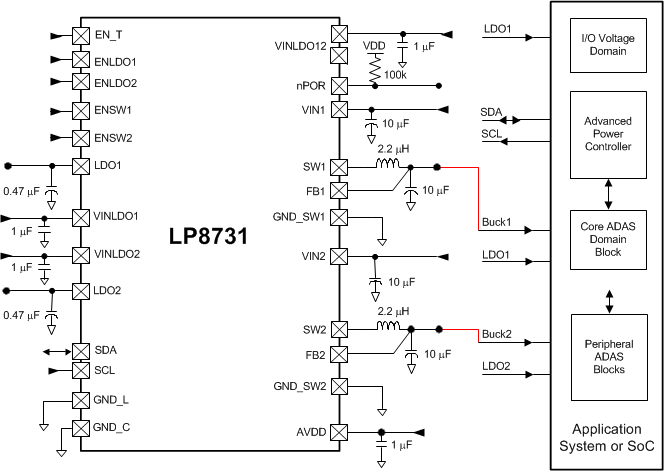
The LP8731-Q1 is a multi-function, programmable Power Management Unit (PMU), optimized for low power FPGAs, microprocessors, and DSPs. This device integrates two highly efficient 1.2-A step-down DC-DC converters with dynamic voltage management (DVM), two 300-mA linear regulators, and a 400-kHz I2C-compatible interface to allow a host controller access to the internal control registers of the LP8731-Q1. The LP8731-Q1 device additionally features programmable power-on sequencing.
Device Information(1)
| PART NUMBER | PACKAGE | BODY SIZE (MAX) |
|---|---|---|
| LP8731-Q1 | DSBGA (25) | 2.52 mm x 2.52 mm |
- For all available packages, see the orderable addendum at the end of the datasheet.
Simplified Schematic

4 Revision History
| DATE | REVISION | NOTES |
|---|---|---|
| December 2014 | * | Initial release. |