SLOS931A November 2015 – November 2015 OPA1612-Q1
PRODUCTION DATA.
- 1 Features
- 2 Applications
- 3 Description
- 4 Revision History
- 5 Pin Configuration and Functions
- 6 Specifications
- 7 Parameter Measurement Information
- 8 Detailed Description
- 9 Application and Implementation
- 10Power-Supply Recommendations
- 11Layout
- 12Device and Documentation Support
- 13Mechanical, Packaging, and Orderable Information
Package Options
Mechanical Data (Package|Pins)
- D|8
Thermal pad, mechanical data (Package|Pins)
Orderable Information
1 Features
- Qualified for Automotive Applications
- AEC-Q100 Qualified With the Following Results:
- Device Temperature Grade 1: –40°C to +125°C Ambient Operating Temperature Range
- Device HBM Classification Level 2
- Device CDM Classification Level C6
- Superior Sound Quality
- Ultralow Noise: 1.1 nV/√Hz at 1 kHz
- Ultralow Distortion:
0.000015% at 1 kHz - High Slew Rate: 27 V/μs
- Wide Bandwidth: 40 MHz (G = +1)
- High Open-Loop Gain: 130 dB
- Unity Gain Stable
- Low Quiescent Current:
3.6 mA per Channel - Rail-to-Rail Output
- Wide Supply Range: ±2.25 V to ±18 V
2 Applications
- Professional Audio Equipment
- Microphone Preamplifiers
- Analog and Digital Mixing Consoles
- Broadcast Studio Equipment
- Audio Test And Measurement
- High-End A/V Receivers
3 Description
The OPA1612-Q1 device is a dual, SoundPlus™, bipolar-input operational amplifierthat achieves achieve very low 1.1-nV/√Hz noise density with an ultralow distortion of 0.000015% at 1 kHz. The OPA1612-Q1 device offers rail-to-rail output swing to within 600 mV with a 2-kΩ load, which increases headroom and maximizes dynamic range. These devices also have a high output drive capability of ±30 mA.
These devices operate over a very wide supply range of ±2.25 V to ±18 V, on only 3.6 mA of supply current per channel. The OPA1612-Q1 op amp is unity-gain stable and provide excellent dynamic behavior over a wide range of load conditions.
The dual version features completely independent circuitry for lowest crosstalk and freedom from interactions between channels, even when overdriven or overloaded.
The OPA1612-Q1 device is available in a SOIC-8 package. The device is specified from –40°C to +125°C.
Device Information(1)
| PART NUMBER | PACKAGE | BODY SIZE (NOM) |
|---|---|---|
| OPA1612-Q1 | SOIC (8) | 4.90 mm × 3.91 mm |
- For all available packages, see the orderable addendum at the end of the datasheet.
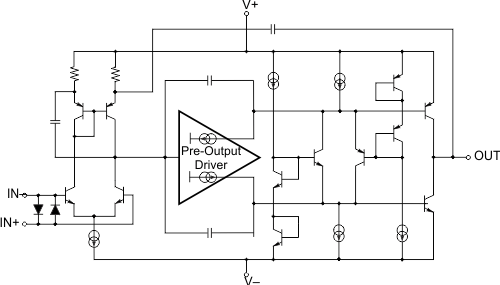
Functional Block Diagram

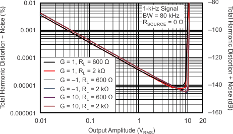
THD+N Ratio vs Output Amplitude
