The OPA314 family of single-, dual-, and quad-channel operational amplifiers represents a new generation of low-power, general-purpose CMOS amplifiers. Rail-to-rail input and output swings, low quiescent current (150 μA typically at 5 VS) combined with a wide bandwidth of 3 MHz, and very low noise (14 nV/√Hz at 1 kHz) make this family very attractive for a variety of battery-powered applications that require a good balance between cost and performance. The low input bias current supports applications with MΩ source impedances.
The robust design of the OPA314 devices provides ease-of-use to the circuit designer: unity-gain stability with capacitive loads of up to 300 pF, an integrated RF/EMI rejection filter, no phase reversal in overdrive conditions, and high electrostatic discharge (ESD) protection (4-kV HBM).
These devices are optimized for low-voltage operation as low as 1.8 V (±0.9 V) and up to 5.5 V (±2.75 V), and are specified over the full extended temperature range of –40°C to 125°C.
The OPA314 (single) is available in both SC70-5 and SOT23-5 packages. The OPA2314 (dual) is offered in SO-8, MSOP-8, and DFN-8 packages. The quad-channel OPA4314 is offered in a TSSOP-14 package.
PART NUMBER | PACKAGE | BODY SIZE (NOM) |
---|---|---|
OPA314 | SOT-23 (5) | 2.90 mm × 1.60 mm |
SC70 (5) | 2.00 mm × 1.25 mm | |
OPA2314 | VSSOP (8) | 3.00 mm × 3.00 mm |
SOIC (8) | 4.90 mm × 3.91 mm | |
VSON (8) | 3.00 mm × 3.00 mm | |
OPA4314 | TSSOP (14) | 5.00 mm × 4.40 mm |
Changes from F Revision (April 2013) to G Revision
Changes from E Revision (September 2012) to F Revision
Changes from D Revision (March 2012) to E Revision
Changes from C Revision (February 2012) to D Revision
Changes from B Revision (December 2011) to C Revision
Changes from A Revision (August 2011) to B Revision
PIN | I/O | DESCRIPTION | ||
---|---|---|---|---|
NAME | DBV | DCK | ||
+IN | 3 | 1 | I | Noninverting input |
–IN | 4 | 3 | I | Inverting input |
OUT | 1 | 4 | O | Output |
V+ | 5 | 5 | — | Positive (highest) supply |
V– | 2 | 2 | — | Negative (lowest) supply |
PIN | I/O | DESCRIPTION | |||
---|---|---|---|---|---|
NAME | DRB | DGK | D | ||
+IN A | 3 | 3 | 3 | I | Noninverting input |
+IN B | 5 | 5 | 5 | I | Noninverting input |
–IN A | 2 | 2 | 2 | I | Inverting input |
–IN B | 6 | 6 | 6 | I | Inverting input |
OUT A | 1 | 1 | 1 | O | Output |
OUT B | 7 | 7 | 7 | O | Output |
V+ | 8 | 8 | 8 | — | Positive (highest) supply |
V– | 4 | 4 | 4 | — | Negative (lowest) supply |
PIN | I/O | DESCRIPTION | |
---|---|---|---|
NAME | NO. | ||
+IN A | 3 | I | Noninverting input |
+IN B | 5 | I | Noninverting input |
+IN C | 10 | I | Noninverting input |
+IN D | 12 | I | Noninverting input |
–IN A | 2 | I | Inverting input |
–IN B | 6 | I | Inverting input |
–IN C | 9 | I | Inverting input |
–IN D | 13 | I | Inverting input |
OUT A | 1 | O | Output |
OUT B | 7 | O | Output |
OUT C | 8 | O | Output |
OUT D | 14 | O | Output |
V+ | 4 | — | Positive (highest) supply |
V– | 11 | — | Negative (lowest) supply |
MIN | MAX | UNIT | ||
---|---|---|---|---|
Supply voltage | 7 | V | ||
Signal input terminals | Voltage(2) | (V–) – 0.5 | (V+) + 0.5 | V |
Current(2) | –10 | 10 | mA | |
Output short-circuit(3) | Continuous | mA | ||
Operating temperature, TA | –40 | 150 | °C | |
Junction temperature, TJ | °C | |||
Storage temperature, Tstg | –65 | 150 | °C |
VALUE | UNIT | |||
---|---|---|---|---|
V(ESD) | Electrostatic discharge | Human-body model (HBM), per ANSI/ESDA/JEDEC JS-001(1) | ±4000 | V |
Charged-device model (CDM), per JEDEC specification JESD22-C101(2) | ±1000 | |||
Machine model (MM) | ±200 |
MIN | NOM | MAX | UNIT | ||
---|---|---|---|---|---|
VS | Supply voltage | 1.8 (±0.9) | 5.5 (±2.75) | V | |
TA | Ambient operating temperature | –40 | 125 | °C |
THERMAL METRIC(1) | OPA314 | UNIT | |||
---|---|---|---|---|---|
DBV (SOT23) | DCK (SC70) | DRL (SOT553) | |||
5 PINS | 5 PINS | 5 PINS | |||
RθJA | Junction-to-ambient thermal resistance | 228.5 | 281.4 | 208.1 | °C/W |
RθJC(top) | Junction-to-case(top) thermal resistance | 99.1 | 91.6 | 0.1 | °C/W |
RθJB | Junction-to-board thermal resistance | 54.6 | 59.6 | 42.4 | °C/W |
ψJT | Junction-to-top characterization parameter | 7.7 | 1.5 | 0.5 | °C/W |
ψJB | Junction-to-board characterization parameter | 53.8 | 58.8 | 42.2 | °C/W |
THERMAL METRIC(1) | OPA2314 | UNIT | |||
---|---|---|---|---|---|
D (SO) | DGK (MSOP) | DRB (DFN) | |||
8 PINS | 8 PINS | 8 PINS | |||
RθJA | Junction-to-ambient thermal resistance | 138.4 | 191.2 | 53.8 | °C/W |
RθJC(top) | Junction-to-case(top) thermal resistance | 89.5 | 61.9 | 69.2 | °C/W |
RθJB | Junction-to-board thermal resistance | 78.6 | 111.9 | 20.1 | °C/W |
ψJT | Junction-to-top characterization parameter | 29.9 | 5.1 | 3.8 | °C/W |
ψJB | Junction-to-board characterization parameter | 78.1 | 110.2 | 11.6 | °C/W |
THERMAL METRIC(1) | OPA4314 | UNIT | ||
---|---|---|---|---|
D (SOIC) | PW (TSSOP) | |||
14 PINS | 14 PINS | |||
RθJA | Junction-to-ambient thermal resistance | 93.2 | 121 | °C/W |
RθJC(top) | Junction-to-case(top) thermal resistance | 51.8 | 49.4 | °C/W |
RθJB | Junction-to-board thermal resistance | 49.4 | 62.8 | °C/W |
ψJT | Junction-to-top characterization parameter | 13.5 | 5.9 | °C/W |
ψJB | Junction-to-board characterization parameter | 42.2 | 62.2 | °C/W |
PARAMETER | TEST CONDITIONS | TA = 25 °C | TA = –40°C to 125°C | UNIT | ||||||
---|---|---|---|---|---|---|---|---|---|---|
MIN | TYP | MAX | MIN | TYP | MAX | |||||
OFFSET VOLTAGE | ||||||||||
VOS | Input offset voltage | VCM = (VS+) – 1.3 V | 0.5 | 2.5 | mV | |||||
dVOS/dT | vs Temperature | 1 | μV/°C | |||||||
PSRR | vs power supply | VCM = (VS+) – 1.3 V | 78 | 92 | dB | |||||
Over temperature | 74 | dB | ||||||||
Channel separation, DC | At DC | 10 | µV/V | |||||||
INPUT VOLTAGE RANGE | ||||||||||
VCM | Common-mode voltage range | (V–) – 0.2 | (V+) + 0.2 | V | ||||||
CMRR | Common-mode rejection ratio | VS = 1.8 V to 5.5 V, (VS–) – 0.2 V < VCM < (VS+) – 1.3 V | 75 | 96 | dB | |||||
VS = 5.5 V, VCM = –0.2 V to 5.7 V(2) | 66 | 80 | dB | |||||||
Over temperature | VS = 1.8 V, (VS–) – 0.2 V < VCM < (VS+) – 1.3 V | 70 | 86 | dB | ||||||
VS = 5.5 V, (VS–) – 0.2 V < VCM < (VS+) – 1.3 V | 73 | 90 | dB | |||||||
VS = 5.5 V, VCM = –0.2 V to 5.7 V(2) | 60 | dB | ||||||||
INPUT BIAS CURRENT | ||||||||||
IB | Input bias current | ±0.2 | ±10 | pA | ||||||
Over temperature | ±600 | pA | ||||||||
IOS | Input offset current | ±0.2 | ±10 | pA | ||||||
Over temperature | ±600 | pA | ||||||||
NOISE | ||||||||||
Input voltage noise (peak-to-peak) | f = 0.1 Hz to 10 Hz | 5 | μVPP | |||||||
en | Input voltage noise density | f = 10 kHz | 13 | nV/√Hz | ||||||
f = 1 kHz | 14 | nV/√Hz | ||||||||
in | Input current noise density | f = 1 kHz | 5 | fA/√Hz | ||||||
INPUT CAPACITANCE | ||||||||||
CIN | Differential | VS = 5 V | 1 | pF | ||||||
Common-mode | VS = 5 V | 5 | pF | |||||||
OPEN-LOOP GAIN | ||||||||||
AOL | Open-loop voltage gain | VS = 1.8 V, 0.2 V < VO < (V+) – 0.2 V, RL = 10 kΩ | 90 | 115 | dB | |||||
VS = 5.5 V, 0.2 V < VO < (V+) – 0.2 V, RL = 10 kΩ | 100 | 128 | dB | |||||||
VS = 1.8 V, 0.5 V < VO < (V+) – 0.5 V, RL = 2 kΩ(2) | 90 | 100 | dB | |||||||
VS = 5.5 V, 0.5 V < VO < (V+) – 0.5 V, RL = 2 kΩ(2) | 94 | 110 | dB | |||||||
Over temperature | VS = 5.5 V, 0.2 V < VO < (V+) – 0.2 V, RL = 10 kΩ | 90 | 110 | dB | ||||||
VS = 5.5 V, 0.5 V < VO < (V+) – 0.2 V, RL = 2 kΩ | 100 | dB | ||||||||
Phase margin | VS = 5 V, G = 1, RL = 10 kΩ | 65 | ° | |||||||
FREQUENCY RESPONSE | ||||||||||
GBW | Gain-bandwidth product | VS = 1.8 V, RL = 10 kΩ, CL = 10 pF | 2.7 | MHz | ||||||
VS = 5 V, RL = 10 kΩ, CL = 10 pF | 3 | MHz | ||||||||
SR | Slew rate(3) | VS = 5 V, G = 1 | 1.5 | V/μs | ||||||
tS | Settling time | To 0.1%, VS = 5 V, 2-V step , G = 1 | 2.3 | μs | ||||||
To 0.01%, VS = 5 V, 2-V step , G = 1 | 3.1 | μs | ||||||||
Overload recovery time | VS = 5 V, VIN × Gain > VS | 5.2 | μs | |||||||
THD+N | Total harmonic distortion + noise(4) | VS = 5 V, VO = 1 VRMS, G = +1, f = 1 kHz, RL = 10 kΩ | 0.001% | |||||||
OUTPUT | ||||||||||
VO | Voltage output swing from supply rails | VS = 1.8 V, RL = 10 kΩ | 5 | 15 | mV | |||||
VS = 5.5 V, RL = 10 kΩ | 5 | 20 | mV | |||||||
VS = 1.8 V, RL = 2 kΩ | 15 | 30 | mV | |||||||
VS = 5.5 V, RL = 2 kΩ | 22 | 40 | mV | |||||||
Over temperature | VS = 5.5 V, RL = 10 kΩ | 30 | mV | |||||||
VS = 5.5 V, RL = 2 kΩ | 60 | mV | ||||||||
ISC | Short-circuit current | VS = 5 V | ±20 | mA | ||||||
RO | Open-loop output impedance | VS = 5.5 V, f = 100 Hz | 570 | Ω | ||||||
POWER SUPPLY | ||||||||||
VS | Specified voltage range | 1.8 | 5.5 | V | ||||||
IQ | Quiescent current per amplifier | OPA314, OPA2314, OPA4314, VS = 1.8 V, IO = 0 mA | 130 | 180 | µA | |||||
OPA2314, OPA4314, VS = 5 V, IO = 0 mA | 150 | 190 | µA | |||||||
OPA314, VS = 5 V, IO = 0 mA | 150 | 210 | µA | |||||||
Over temperature | VS = 5 V, IO = 0 mA | 220 | µA | |||||||
Power-on time | VS = 0 V to 5 V, to 90% IQ level | 44 | µs | |||||||
TEMPERATURE | ||||||||||
Specified range | –40 | 125 | °C | |||||||
Operating range | –40 | 150 | °C | |||||||
Storage range | –65 | 150 | °C |
TITLE | FIGURE |
---|---|
Open-Loop Gain and Phase vs Frequency | Figure 1 |
Open-Loop Gain vs Temperature | Figure 2 |
Quiescent Current vs Supply Voltage | Figure 3 |
Quiescent Current vs Temperature | Figure 4 |
Offset Voltage Production Distribution | Figure 5 |
Offset Voltage Drift Distribution | Figure 6 |
Offset Voltage vs Common-Mode Voltage (Maximum Supply) | Figure 7 |
Offset Voltage vs Temperature | Figure 8 |
CMRR and PSRR vs Frequency (RTI) | Figure 9 |
CMRR and PSRR vs Temperature | Figure 10 |
0.1-Hz to 10-Hz Input Voltage Noise (5.5 V) | Figure 11 |
Input Voltage Noise Spectral Density vs Frequency (1.8 V, 5.5 V) | Figure 12 |
Input Voltage Noise vs Common-Mode Voltage (5.5 V) | Figure 13 |
Input Bias and Offset Current vs Temperature | Figure 14 |
Open-Loop Output Impedance vs Frequency | Figure 15 |
Maximum Output Voltage vs Frequency and Supply Voltage | Figure 16 |
Output Voltage Swing vs Output Current (over Temperature) | Figure 17 |
Closed-Loop Gain vs Frequency, G = 1, –1, 10 (1.8 V) | Figure 18 |
Closed-Loop Gain vs Frequency, G = 1, –1, 10 (5.5 V) | Figure 19 |
Small-Signal Overshoot vs Load Capacitance | Figure 20 |
Small-Signal Step Response, Noninverting (1.8 V) | Figure 21 |
Small-Signal Step Response, Noninverting ( 5.5 V) | Figure 22 |
Large-Signal Step Response, Noninverting (1.8 V) | Figure 23 |
Large-Signal Step Response, Noninverting ( 5.5 V) | Figure 24 |
Positive Overload Recovery | Figure 25 |
Negative Overload Recovery | Figure 26 |
No Phase Reversal | Figure 27 |
Channel Separation vs Frequency (Dual) | Figure 28 |
THD+N vs Amplitude (G = 1, 2 kΩ, 10 kΩ) | Figure 29 |
THD+N vs Amplitude (G = –1, 2 kΩ, 10 kΩ) | Figure 30 |
THD+N vs Frequency (0.5 VRMS, G = +1, 2 kΩ, 10 kΩ) | Figure 31 |
EMIRR | Figure 32 |
The OPA314 is a family of low-power, rail-to-rail input and output operational amplifiers specifically designed for portable applications. These devices operate from 1.8 V to 5.5 V, are unity-gain stable, and suitable for a wide range of general-purpose applications. The class AB output stage is capable of driving ≤ 10-kΩ loads connected to any point between V+ and ground. The input common-mode voltage range includes both rails, and allows the OPA314 series to be used in virtually any single-supply application. Rail-to-rail input and output swing significantly increases dynamic range, especially in low-supply applications, and makes them ideal for driving sampling analog-to-digital converters (ADCs).
The OPA314 features 3-MHz bandwidth and 1.5-V/μs slew rate with only 150-μA supply current per channel, providing good AC performance at very low power consumption. DC applications are also well served with a very low input noise voltage of 14 nV/√Hz at 1 kHz, low input bias current (0.2 pA), and an input offset voltage of 0.5 mV (typical).
The OPA314 series operational amplifiers are fully specified and ensured for operation from 1.8 V to 5.5 V. In addition, many specifications apply from –40°C to 125°C. Parameters that vary significantly with operating voltages or temperature are shown in the Typical Characteristics graphs. Power-supply pins should be bypassed with 0.01-μF ceramic capacitors.
The input common-mode voltage range of the OPA314 series extends 200 mV beyond the supply rails. This performance is achieved with a complementary input stage: an N-channel input differential pair in parallel with a P-channel differential pair, as shown in Figure 33. The N-channel pair is active for input voltages close to the positive rail, typically (V+) – 1.3 V to 200 mV above the positive supply, while the P-channel pair is on for inputs from 200 mV below the negative supply to approximately (V+) – 1.3 V. There is a small transition region, typically (V+) – 1.4 V to (V+) – 1.2 V, in which both pairs are on. This 200-mV transition region can vary up to 300 mV with process variation. Thus, the transition region (both stages on) can range from (V+) – 1.7 V to (V+) – 1.5 V on the low end, up to (V+) – 1.1 V to (V+) – 0.9 V on the high end. Within this transition region, PSRR, CMRR, offset voltage, offset drift, and THD may be degraded compared to device operation outside this region.
The OPA314 family incorporates internal electrostatic discharge (ESD) protection circuits on all pins. In the case of input and output pins, this protection primarily consists of current-steering diodes connected between the input and power-supply pins. These ESD protection diodes also provide in-circuit, input overdrive protection, as long as the current is limited to 10 mA as stated in the Absolute Maximum Ratings. Figure 34 shows how a series input resistor may be added to the driven input to limit the input current. The added resistor contributes thermal noise at the amplifier input and its value should be kept to a minimum in noise-sensitive applications.
CMRR for the OPA314 is specified in several ways so the best match for a given application may be used; see the Electrical Characteristics. First, the CMRR of the device in the common-mode range below the transition region [VCM < (V+) – 1.3 V] is given. This specification is the best indicator of the capability of the device when the application requires use of one of the differential input pairs. Second, the CMRR over the entire common-mode range is specified at (VCM = –0.2 V to 5.7 V). This last value includes the variations seen through the transition region (see Figure 7).
Operational amplifiers vary with regard to the susceptibility of the device to electromagnetic interference (EMI). If conducted EMI enters the operational amplifier, the DC offset observed at the amplifier output may shift from its nominal value while EMI is present. This shift is a result of signal rectification associated with the internal semiconductor junctions. While all operational amplifier pin functions can be affected by EMI, the signal input pins are likely to be the most susceptible. The OPA314 operational amplifier family incorporate an internal input low-pass filter that reduces the amplifiers response to EMI. Both common-mode and differential mode filtering are provided by this filter. The filter is designed for a cutoff frequency of approximately 80 MHz (–3 dB), with a roll-off of 20 dB per decade.
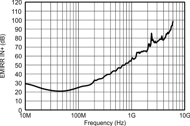
Texas Instruments has developed the ability to accurately measure and quantify the immunity of an operational amplifier over a broad frequency spectrum extending from 10 MHz to 6 GHz. The EMI rejection ratio (EMIRR) metric allows operational amplifiers to be directly compared by the EMI immunity. Figure 32 illustrates the results of this testing on the OPAx314. Detailed information can also be found in the application report, EMI Rejection Ratio of Operational Amplifiers (SBOA128), available for download from www.ti.com.
Designed as a micro-power, low-noise operational amplifier, the OPA314 delivers a robust output drive capability. A class AB output stage with common-source transistors is used to achieve full rail-to-rail output swing capability. For resistive loads up to 10 kΩ, the output swings typically to within 5 mV of either supply rail regardless of the power-supply voltage applied. Different load conditions change the ability of the amplifier to swing close to the rails; refer to Figure 17.
The OPA314 is designed to be used in applications where driving a capacitive load is required. As with all operational amplifiers, there may be specific instances where the OPA314 can become unstable. The particular operational amplifiers circuit configuration, layout, gain, and output loading are some of the factors to consider when establishing whether or not an amplifier is stable in operation. An operational amplifier in the unity-gain (+1-V/V) buffer configuration that drives a capacitive load exhibits a greater tendency to be unstable than an amplifier operated at a higher noise gain. The capacitive load, in conjunction with the operational amplifier output resistance, creates a pole within the feedback loop that degrades the phase margin. The degradation of the phase margin increases as the capacitive loading increases. When operating in the unity-gain configuration, the OPA314 remains stable with a pure capacitive load up to approximately 1 nF. The equivalent series resistance (ESR) of some very large capacitors (CL greater than 1 μF) is sufficient to alter the phase characteristics in the feedback loop such that the amplifier remains stable. Increasing the amplifier closed-loop gain allows the amplifier to drive increasingly larger capacitance. This increased capability is evident when observing the overshoot response of the amplifier at higher voltage gains. See Figure 20.
One technique for increasing the capacitive load drive capability of the amplifier operating in a unity-gain configuration is to insert a small resistor, typically 10 Ω to 20 Ω, in series with the output, as shown in Figure 35. This resistor significantly reduces the overshoot and ringing associated with large capacitive loads. One possible problem with this technique, however, is that a voltage divider is created with the added series resistor and any resistor connected in parallel with the capacitive load. The voltage divider introduces a gain error at the output that reduces the output swing.
The OPA2314 device is powered on when the supply is connected. The device can be operated as a single-supply operational amplifier or a dual-supply amplifier, depending on the application.
NOTE
Information in the following applications sections is not part of the TI component specification, and TI does not warrant its accuracy or completeness. TI’s customers are responsible for determining suitability of components for their purposes. Customers should validate and test their design implementation to confirm system functionality.
The OPA2314 device is a low-power, rail-to-rail input and output operational amplifier specifically designed for portable applications. The device operates from 1.8 V to 5.5 V, is unity-gain stable, and suitable for a wide range of general-purpose applications. The class AB output stage is capable of driving ≤ 10-kΩ loads connected to any point between V+ and ground. The input common-mode voltage range includes both rails, and allows the OPA2314 device to be used in virtually any single-supply application. Rail-to-rail input and output swing significantly increases dynamic range, especially in low-supply applications, and makes the device ideal for driving sampling analog-to-digital converters (ADCs).
The OPA2314 device features a 3-MHz bandwidth and 1.5-V/μs slew rate with only 150-μA supply current per channel, providing good AC performance at very low power consumption. DC applications are also well served with a very-low input noise voltage of 14 nV/√Hz at 1 kHz, low-input bias current (0.2 pA), and an input offset voltage of 0.5 mV (typical).
When receiving low-level signals, limiting the bandwidth of the incoming signals into the system is often required. The simplest way to establish this limited bandwidth is to place an RC filter at the noninverting terminal of the amplifier, as Figure 36 shows.
If even more attenuation is needed, a multiple pole filter is required. The Sallen-Key filter can be used for this task, as Figure 37 shows. For best results, the amplifier should have a bandwidth that is eight to 10 times the filter frequency bandwidth. Failure to follow this guideline can result in phase shift of the amplifier.
The OPA2314 device is designed to be used in applications where driving a capacitive load is required. As with all op-amps, specific instances can occur where the OPA2314 device can become unstable. The particular op-amp circuit configuration, layout, gain, and output loading are some of the factors to consider when establishing whether or not an amplifier is stable in operation. An op-amp in the unity-gain (1 V/V) buffer configuration that drives a capacitive load exhibits a greater tendency to be unstable than an amplifier operated at a higher noise gain. The capacitive load, in conjunction with the op-amp output resistance, creates a pole within the feedback loop that degrades the phase margin. The degradation of the phase margin increases as the capacitive loading increases. When operating in the unity-gain configuration, the OPA2314 device remains stable with a pure capacitive load up to approximately 1 nF. The equivalent series resistance (ESR) of some very large capacitors (CL greater than 1 μF) is sufficient to alter the phase characteristics in the feedback loop such that the amplifier remains stable. Increasing the amplifier closed-loop gain allows the amplifier to drive increasingly larger capacitance. This increased capability is evident when observing the overshoot response of the amplifier at higher voltage gains. See the graph, Figure 20.
One technique for increasing the capacitive load drive capability of the amplifier operating in a unity-gain configuration is to insert a small resistor, typically 10 Ω to 20 Ω, in series with the output, as shown in Figure 38. This resistor significantly reduces the overshoot and ringing associated with large capacitive loads. One possible problem with this technique, however, is that a voltage divider is created with the added series resistor and any resistor connected in parallel with the capacitive load. The voltage divider introduces a gain error at the output that reduces the output swing.
Some applications require differential signals. Figure 39 shows a simple circuit to convert a single-ended input of 0.1 V to 2.4 V into a differential output of ±2.3 V on a single 2.7-V supply. The output range is intentionally limited to maximize linearity. The circuit is composed of two amplifiers. One amplifier functions as a buffer and creates a voltage, VOUT+. The second amplifier inverts the input and adds a reference voltage to generate VOUT–. Both VOUT+ and VOUT– range from 0.1 V to 2.4 V. The difference, VDIFF, is the difference between VOUT+ and VOUT–. This makes the differential output voltage range 2.3 V.
The design requirements are as follows:
The circuit in Figure 39 takes a single-ended input signal, VIN, and generates two output signals, VOUT+ and VOUT– using two amplifiers and a reference voltage, VREF. VOUT+ is the output of the first amplifier and is a buffered version of the input signal, VIN (as shown in Equation 1). VOUT– is the output of the second amplifier which uses VREF to add an offset voltage to VIN and feedback to add inverting gain. The transfer function for VOUT– is given in Equation 2.
The differential output signal, VDIFF, is the difference between the two single-ended output signals, VOUT+ and VOUT–. Equation 3 shows the transfer function for VDIFF. By applying the conditions that R1 = R2 and R3 = R4, the transfer function is simplified into Equation 6. Using this configuration, the maximum input signal is equal to the reference voltage and the maximum output of each amplifier is equal to VREF. The differential output range is 2 × VREF. Furthermore, the common-mode voltage is one half of VREF (see Equation 7).
Linearity over the input range is key for good dc accuracy. The common-mode input range and output swing limitations determine the linearity. In general, an amplifier with rail-to-rail input and output swing is required. Bandwidth is a key concern for this design, so the OPA2314-Q1 device is selected because its bandwidth is greater than the target of 1 MHz. The bandwidth and power ratio makes this device power efficient and the low offset and drift ensure good accuracy for moderate precision applications.
Because the transfer function of Vout– is heavily reliant on resistors (R1, R2, R3, and R4), use resistors with low tolerances to maximize performance and minimize error. This design uses resistors with resistance values of 49.9 kΩ and tolerances of 0.1%. However, if the noise of the system is a key parameter, smaller resistance values (6 kΩ or lower) can be selected to keep the overall system noise low. This ensures that the noise from the resistors is lower than the amplifier noise.
The OPA2314-Q1 device is specified for operation from 1.8 V to 5.5 V (±0.9 V to ±2.75 V); many specifications apply from –40°C to 125°C. The Typical Characteristics presents parameters that can exhibit significant variance with regard to operating voltage or temperature.
CAUTION
Supply voltages larger than 7 V can permanently damage the device (see the Absolute Maximum Ratings).
Place 0.1-μF bypass capacitors close to the power-supply pins to reduce errors coupling in from noisy or high-impedance power supplies. For more detailed information on bypass capacitor placement, refer to the Layout Guidelines section.