SBOS303D June 2004 – December 2016 OPA820
PRODUCTION DATA.
- 1 Features
- 2 Applications
- 3 Description
- 4 Revision History
- 5 Device Comparison Table
- 6 Pin Configuration and Functions
- 7 Specifications
- 8 Parameter Measurement Information
- 9 Detailed Description
- 10Application and Implementation
- 11Power Supply Recommendations
- 12Layout
- 13Device and Documentation Support
- 14Mechanical, Packaging, and Orderable Information
Package Options
Refer to the PDF data sheet for device specific package drawings
Mechanical Data (Package|Pins)
- D|8
- DBV|5
Thermal pad, mechanical data (Package|Pins)
Orderable Information
1 Features
- High Bandwidth (240 MHz, G = 2)
- High-Output Current (±110 mA)
- Low-Input Noise (2.5 nV/√Hz)
- Low-Supply Current (5.6 mA)
- Flexible Supply Voltage:
- Dual ±2.5 V to ±6 V
- Single 5 V to 12 V
- Excellent DC Accuracy:
- Maximum 25°C Input Offset Voltage = ±750 µV
- Maximum 25°C Input Offset Current = ±400 nA
2 Applications
- Low-Cost Video Line Drivers
- ADC Preamplifiers
- Active Filters
- Low-Noise Integrators
- Portable Test Equipment
- Optical Channel Amplifiers
- Low-Power, Baseband Amplifiers
- CCD Imaging Channel Amplifiers
- OPA650 and OPA620 Upgrade
3 Description
The OPA820 device provides a wideband, unity-gain stable, voltage-feedback amplifier with a very-low input-noise voltage and high-output current using a low 5.6-mA supply current. At unity-gain, the OPA820 device gives more than 800-MHz bandwidth with less than 1-dB peaking. The OPA820 device complements this high-speed operation with excellent DC precision in a low-power device. A worst-case input-offset voltage of ±750 µV and an offset current of ±400 nA provide excellent absolute DC precision for pulse amplifier applications.
Minimal input and output voltage-swing headroom allow the OPA820 device to operate on a single 5-V supply with more than 2-VPP output swing. While not a rail-to-rail (RR) output, this swing supports most emerging analog-to-digital converter (ADC) input ranges with lower power and noise than typical RR output op amps.
Exceptionally low dG/dP (0.01% or 0.03°) supports low-cost composite-video line-driver applications. Existing designs can use the industry-standard pinout, 8-pin SOIC package while emerging high-density portable applications can use the 5-pin SOT-23. Offering the lowest thermal impedance of the industry in a SOT package, along with full specification over both the commercial and industrial temperature ranges, provides solid performance over a wide temperature range.
Device Information(1)
| PART NUMBER | PACKAGE | BODY SIZE (NOM) |
|---|---|---|
| OPA820 | SOIC (8) | 4.90 mm × 3.91 mm |
| SOT-23 (5) | 2.90 mm × 1.60 mm |
- For all available packages, see the orderable addendum at the end of the data sheet.
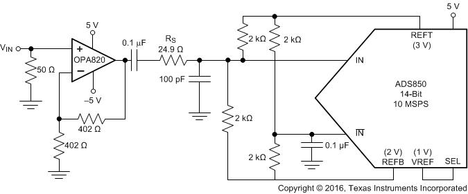
AC-Coupled, 14-Bit ADS850 Interface
